Design Linked Incentive Scheme: India’s Semiconductor Design Push
A January 2026 PIB backgrounder put the Design Linked Incentive scheme back in focus as part of India’s semiconductor strategy. The DLI scheme supports chip design, intellectual property and domestic fabless semiconductor companies.
For UPSC, this topic matters because semiconductors are now industrial policy, national security, trade policy and science policy at the same time. India cannot build a credible electronics ecosystem by focusing only on assembly.
This article explains why chip design is strategically different from chip fabrication and how DLI fits into India’s semiconductor mission.
Quick Facts
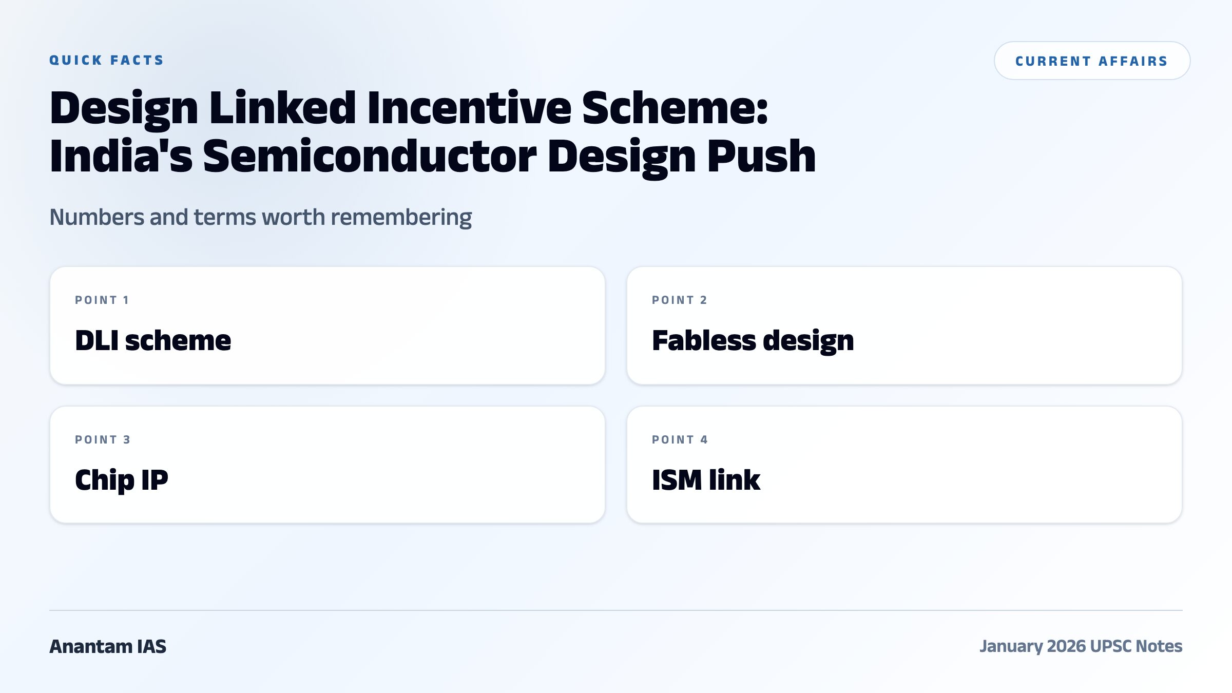
- DLI stands for Design Linked Incentive.
- It supports semiconductor design, IP cores and fabless chip companies.
- The scheme is part of the India Semiconductor Mission ecosystem.
- Semiconductor design is less capital-intensive than fabrication but deeply talent-intensive.
- Chips are critical for telecom, defence, AI, automobiles, electronics and energy systems.
- Official source: PIB January 2026 backgrounder on DLI.
- Official source: PIB backgrounder.
What Just Happened
The January 2026 official backgrounder highlighted the DLI scheme as a pillar of India’s semiconductor policy.
The update is important because India’s semiconductor conversation often focuses on fabs. Design capability is equally strategic because it captures intellectual property and high-value engineering.
For aspirants, DLI is a way to connect PLI-style industrial policy with technological sovereignty and global supply-chain resilience.
Background and Historical Context
The global semiconductor industry is organised across design, electronic design automation, fabrication, packaging, testing and end-use manufacturing. No country dominates every layer equally.
India has strong chip-design talent through global capability centres and engineering services, but domestic ownership of product IP has been weaker.
The India Semiconductor Mission seeks to build a more complete ecosystem through incentives for fabs, display manufacturing, compound semiconductors, design and talent.
Key Features of Semiconductor Policy
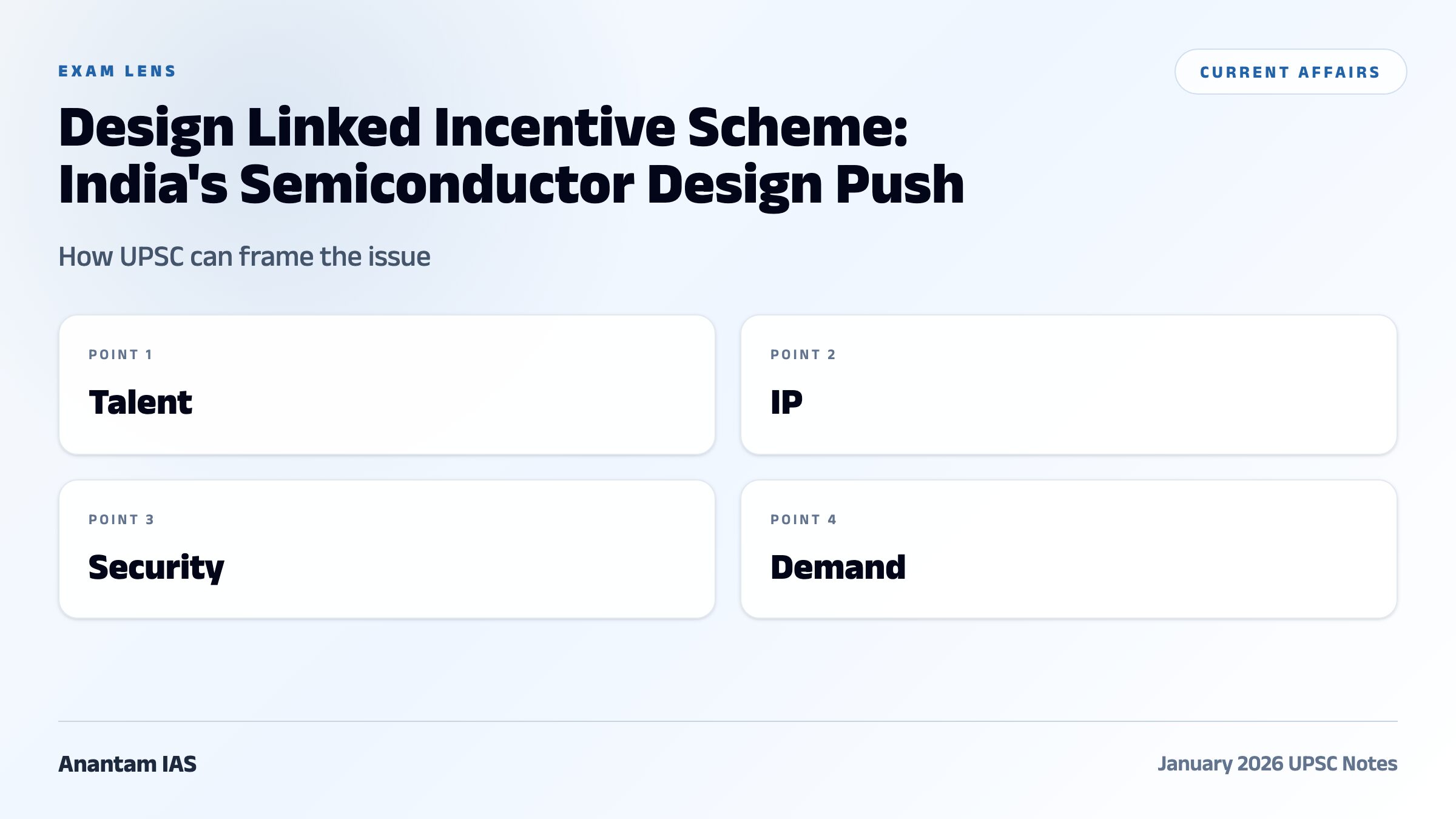
The core policy architecture can be read through these features.
- Fabless focus: DLI supports companies that design chips but outsource fabrication.
- IP creation: the goal is Indian-owned design intellectual property.
- Financial support: incentives reduce early-stage design and prototype costs.
- Talent leverage: India can use its engineering workforce before full fab depth emerges.
- Strategic sectors: telecom, defence, automotive and AI need trusted chips.
- Ecosystem link: design must connect with packaging, testing, fabs and end customers.
Why It Matters
This is a high-yield UPSC topic because it joins current news with durable syllabus themes.
- It connects a January 2026 event with durable UPSC syllabus themes.
- It gives usable facts for Prelims and analytical hooks for Mains.
- It helps students move from news recall to policy reasoning.
- It can be linked with static concepts in polity, economy, governance, science, environment or society.
Detailed Analysis: Semiconductor Policy Lens
Design is where value and control begin. A country that only assembles electronics depends on others for architecture, security and margins.
Fabs are capital-heavy; design is talent-heavy. India can move faster in design if it supports startups, EDA access, prototyping and market linkages.
The missing bridge is commercial demand. DLI-backed designs must find buyers in telecom, defence, automotive and public procurement ecosystems.
Comparative Perspective
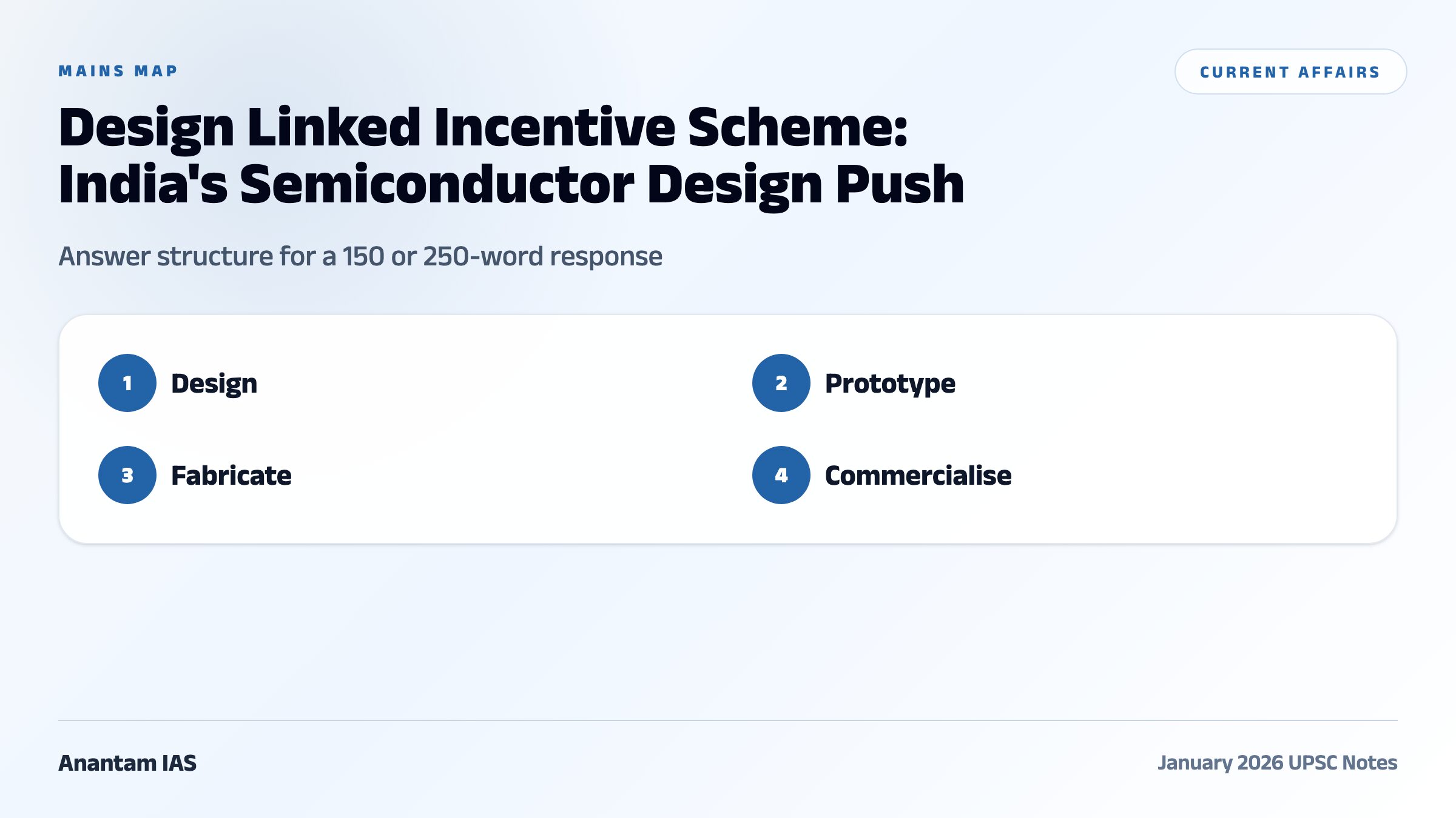
A comparison helps prevent the answer from becoming a one-dimensional news summary.
- Taiwan: fabrication strength through foundries such as TSMC.
- United States: strong in design, EDA tools and advanced chips.
- China: heavy state support across the chip stack despite export controls.
- India: stronger in design talent than fabrication depth, making DLI strategically important.
Challenges
The policy or institutional promise runs into recurring constraints.
- EDA tools and advanced IP blocks are expensive and often foreign-controlled.
- Startups face long product cycles and uncertain buyers.
- Fabrication access for prototypes can be costly.
- Design talent must be retained in domestic product companies.
- Security-sensitive sectors require trusted supply chains and testing standards.
Prelims Pointers
- Fabless companies design chips but do not own fabrication plants.
- EDA means Electronic Design Automation.
- India Semiconductor Mission supports semiconductor and display ecosystem development.
- Semiconductors are essential for electronics, defence, telecom, AI and vehicles.
- Chip fabrication plants are capital-intensive and water/power intensive.
- Design IP can create high-value domestic capability.
Mains Questions
- Why is semiconductor design strategically important for India even before large-scale fabrication matures? (GS Paper III, 250 words)
- Compare design-linked incentives with production-linked incentives in technology sectors. (GS Paper III, 150 words)
- Semiconductor self-reliance requires ecosystem depth, not only fabs. Discuss. (GS Paper III, 250 words)
- How can public procurement support domestic semiconductor design? (GS Paper III, 150 words)
Way Forward
India should support design startups with EDA access, prototyping grants, trusted foundry partnerships and anchor demand from defence, telecom and public digital infrastructure.
DLI must be judged by Indian-owned IP, chips reaching production and startups surviving beyond prototype stage.
For UPSC, remember the layered answer: design, fabrication, packaging, testing, talent and demand all matter.
The examiner is unlikely to reward a bare fact dump here. The better answer connects the January 2026 event to institutional design, implementation capacity and India’s long-term development priorities.
Frequently Asked Questions
What is the DLI scheme?
It is the Design Linked Incentive scheme that supports semiconductor design and domestic chip IP creation.
What is a fabless chip company?
It designs chips but outsources fabrication to a foundry.
Why does chip design matter?
Design captures high-value intellectual property and strategic control over chip architecture.
Is DLI the same as PLI?
No. DLI targets design capability, while PLI usually rewards production output.
Which mission is linked to DLI?
India Semiconductor Mission.
What is the main challenge?
Moving from supported designs to commercial products with buyers and secure supply chains.