Semiconductor Industry – India’s Strategic Tech Frontier
General Studies · Science & Tech
Context: The Union Cabinet has approved four additional semiconductor manufacturing projects under the India Semiconductor Mission (ISM), marking a significant boost to the country’s semiconductor ecosystem.
The new projects come from SiCSem, Continental Device India Private Limited (CDIL), 3D Glass Solutions Inc., and Advanced System in Package (ASIP) Technologies. They will establish semiconductor manufacturing units in Odisha, Punjab, and Andhra Pradesh, addressing growing demands across telecom, automotive, data centres, consumer electronics, and industrial sectors.
UPSC relevance:
GS Paper 1
Factors responsible for the location of primary, secondary, and tertiary sector industries in various parts of the world (including India).
Questions have been regularly asked in mains regarding location factors of various industries:
2022: Describing the distribution of rubber-producing countries indicates their major environmental issues
2021: Discuss the multi-dimensional implications of the uneven distribution of mineral oil in the world.
What are Semiconductors?
Semiconductors are materials whose electrical conductivity lies between that of a conductor and an insulator, enabling their use in microchips and integrated circuits (ICs). Foundation of modern electronics — used in smartphones, automobiles, defense systems, AI, IoT, and 5G.
USD 600+ billion (2023), projected to reach USD 1 trillion by 2030 (McKinsey). India imports 100% of its semiconductors, with an import bill of ~$25 billion annually (Electronics Ministry, 2023).
Global distribution of Semiconductor manufacturing
The semiconductor industry is the aggregate of companies engaged in the design and fabrication of semiconductors and semiconductor devices, such as transistors and integrated circuits. The global semiconductor industry is dominated by companies from the United States, Taiwan, South Korea, Japan and the Netherlands, with Israel and Germany having significant presence in the field.
Factors Influencing Global Location
Example: China’s fab expansion for Huawei, BYD.
Skilled Workforce & R&D Ecosystem
High-end engineering talent, proximity to research hubs.
–Taiwan’s Hsinchu Science Park + National Tsing Hua University.
Case: South Korea’s KAIST–Samsung synergy.
Capital-Intensive Investment Climate
Fabs cost $10–20 billion; need deep capital markets, subsidies.
Strategic Importance – Essential for defense, AI, quantum computing, and cyber security.
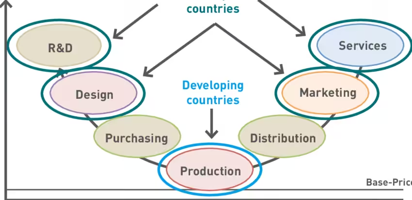
Tech Industry Boost – Move up the Global Value Chain (GVC) smile curve from assembly to design & fabrication.
Employment Generation – High-skill job creation; 5,00,000 jobs projected in ESDM sector.
Tax Revenue Growth – Expansion of formal electronics sector.
Export Potential – Integration into global supply chains; opportunity to supply to automotive & electronics giants.
Import Reduction – Self-reliance in a critical technology domain.
What’s a Smiling curve?
In business management theory, the smiling curve is a graphical depiction of how value added varies across the different stages of bringing a product on to the market in an IT-related manufacturing industry. The concept was first proposed around 1992 by Stan Shih, the founder of Acer Inc., an IT company headquartered in Taiwan.
According to Shih’s observation, in the personal computer industry, the two ends of the value chain – conception and marketing – command higher values added to the product than the middle part of the value chain – manufacturing. If this phenomenon is presented in a graph with a Y-axis for value-added and an X-axis for value chain (stage of production), the resulting curve appears like a “smile”.
Location Factors for Semiconductor Industry in India
Large Domestic Market – 2nd largest internet user base (~880 million users in 2023).
Skilled & Cheap Workforce – Large pool of engineers; India produces ~1.5 million engineers/year.
Capital Access – 100% FDI permitted in electronics manufacturing.
Infrastructure Support – National Infrastructure Pipeline (NIP), electronics clusters.
Government Incentives – Production Linked Incentive (PLI) scheme for semiconductors & display fabs.
Transportation – Port-led connectivity via Sagarmala, dedicated freight corridors.
Challenges for India
Raw Material Dependence – Limited domestic supply of high-purity silicon wafers and rare earths.
High Establishment Cost – Semiconductor fab cost can exceed $10 billion.
Ease of Doing Business Issues – Land acquisition delays, regulatory complexity.
Technological Constraints – Lag in advanced node manufacturing (India has no commercial fabs yet).