

Why in News?
On 15 August 2026, the Ministry of Electronics and Information Technology announced that Chennai-based Aheesa Digital Innovations had achieved first-pass silicon success for VIHAAN, a networking system-on-chip designed for fibre-broadband equipment.
- Aheesa is a fabless semiconductor company: it designs the chip and associated platform but depends on a semiconductor foundry for physical fabrication.
- The VIHAAN design was taped out on 26 January 2026, according to the PIB release, and the fabricated silicon achieved the announced first-pass milestone on 15 August 2026.
- VIHAAN is a purpose-built networking SoC for fibre broadband and uses a 64-bit processor from C-DAC’s indigenous VEGA family, which is based on the open RISC-V instruction set architecture.
- The company says the platform is intended for fibre-to-the-home customer-premises equipment and supports broadband interfaces such as GPON and EPON; these product claims still require customer-level integration and validation before mass deployment.
- PIB reported that Aheesa had raised about ₹40 crore from the Tamil Nadu Emerging Sector Seed Fund and other private investors to support product development and growth.
- Broadband equipment contains specialised silicon for packet processing, security, memory control and optical-access functions. Domestic ownership of the design and intellectual property can improve the scope for local adaptation, security review and value addition.
- Chip design captures a high-value part of the semiconductor chain, but it cannot substitute for fabrication, assembly, packaging, testing, reliable software, customer qualification and volume production.
- The milestone illustrates how public design infrastructure and incentives can reduce the high upfront cost faced by fabless startups, while private finance and OEM demand remain necessary for commercial scale.
UPSC Relevance
Prelims Relevance
- A system-on-chip integrates several computing and system functions, such as processor cores, memory controllers, interfaces and accelerators, on one integrated circuit.
- A fabless company develops semiconductor architecture and designs but contracts fabrication to a foundry; an integrated device manufacturer combines more stages within one company.
- Tape-out is the point at which the final chip-layout data is released for mask preparation and fabrication. It is not the same as receiving or validating fabricated silicon.
- First-pass silicon generally means the first fabricated iteration performs well enough against the developer’s targeted checks to continue development without an immediate full design re-spin. The exact validation scope must be read from the developer’s disclosure.
- A production tape-out is a later design release intended for a manufacturing-ready version; it still precedes fabrication, testing, yield learning and volume production.
- RISC-V is an open-standard instruction set architecture. An open ISA does not automatically make every processor implementation or SoC design open-source.
Mains Relevance
GS Paper 3
- Use VIHAAN as a case study of movement from domestic processor IP and chip design to fabricated silicon in a strategic telecom application.
- Examine the different policy requirements of the semiconductor value chain: design tools and IP, foundry access, packaging and testing, firmware, standards compliance, patient capital and assured demand.
GS Paper 2
- Evaluate the state as an ecosystem builder through the DLI Scheme, C-DAC processor IP, shared electronic-design-automation infrastructure and startup support.
- Discuss how transparent milestone reporting and outcome-based public support can balance strategic autonomy with fiscal accountability.
Essay
- Technological self-reliance is not isolation; it is the capacity to design, verify, adapt and negotiate from a position of capability.
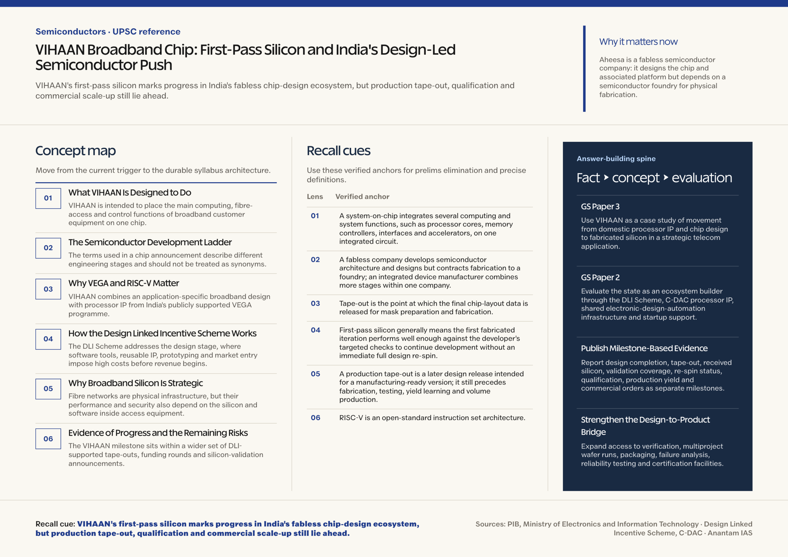
Background and Context
What VIHAAN Is Designed to Do
VIHAAN is intended to place the main computing, fibre-access and control functions of broadband customer equipment on one chip.
- Aheesa describes VIHAAN as a RISC-V networking SoC for fibre-to-the-home customer-premises equipment, where it can support the handling of optical-access traffic and local network connections.
- Its published platform description lists GPON, EPON and Gigabit Ethernet, along with DDR4 memory, SPI NOR Flash and eMMC storage support. These interfaces allow a device maker to combine access-network termination, data processing and system.
- The 2025 MeitY roadmap described VIHAAN as being built around a 64-bit C-DAC VEGA processor, with secure boot, security enhancements, PCIe 3.0 and USB 3.0 among the intended connectivity features.
- The chip is one part of a product stack. Reference hardware, boot software, drivers, an operating system, networking software and OEM testing are also needed before a broadband device reaches users.
The Semiconductor Development Ladder
The terms used in a chip announcement describe different engineering stages and should not be treated as synonyms.
- Design covers architecture, logic, integration of processor and interface IP, verification and the physical layout needed for manufacture.
- At tape-out, the design team freezes and sends the final layout data to a foundry. The foundry then uses that data to prepare masks and fabricate wafers.
- Fabricated dies must be packaged and subjected to electrical, functional and reliability tests. A successful first pass reduces the risk and cost of an immediate redesign, but it does not by itself establish production yield, long-term.
- A design may still change after first silicon as engineers correct issues, improve performance, incorporate test learning or prepare a production version. PIB explicitly says VIHAAN will proceed towards a production tape-out targeted for 2027.
- Commercial readiness requires further gates: stable yields at the foundry, packaging and testing capacity, firmware maturity, reference platforms, standards and operator qualification, supply commitments and customer orders.
Why VEGA and RISC-V Matter
VIHAAN combines an application-specific broadband design with processor IP from India’s publicly supported VEGA programme.
- C-DAC’s VEGA family includes 32-bit and 64-bit single-core and multicore processors based on the RISC-V instruction set architecture, with variants for embedded and higher-performance applications.
- RISC-V provides an open instruction set specification, allowing implementers to design compatible processor cores without depending on a proprietary ISA licence. The surrounding processor core, peripherals, accelerators, software and SoC layout can still contain separately.
- Using domestic processor IP can build local competence in debugging, security review, customisation and lifecycle support. It may also give designers greater control over product roadmaps for strategic or India-specific applications.
- The test of sovereignty is not the label alone. Policymakers should ask which design blocks are locally owned, where fabrication and packaging occur, what tool and foreign-IP dependencies remain, and whether local firms can maintain the.
How the Design Linked Incentive Scheme Works
The DLI Scheme addresses the design stage, where software tools, reusable IP, prototyping and market entry impose high costs before revenue begins.
- The scheme supports domestic companies, startups and MSMEs designing integrated circuits, chipsets, SoCs, systems and semiconductor IP cores through financial incentives and design-infrastructure access.
- Its stated objectives are to nurture domestic design firms, increase Indian-owned semiconductor content and IP, support import substitution and value addition, and improve startup and MSME access to design infrastructure.
- C-DAC is the nodal agency. This creates a policy bridge between publicly developed processor technology, shared design support and private product companies such as Aheesa.
- According to PIB, government semiconductor programmes had made advanced chip-design tools available to 455 organisations, comprising 350 academic institutions and 105 startups. Such access can lower entry barriers, but it does not remove the need.
Way Forward
Publish Milestone-Based Evidence
- Report design completion, tape-out, received silicon, validation coverage, re-spin status, qualification, production yield and commercial orders as separate milestones.
- Use independently auditable indicators while protecting genuine trade secrets and security-sensitive design details.
- Track domestic ownership of IP, value addition, skilled employment, exports and long-term product support alongside the number of supported firms.
Conclusion
- VIHAAN’s first-pass silicon is a credible engineering milestone because it shows that an Indian fabless company has carried a broadband SoC from design and tape-out to fabricated hardware that can enter deeper validation.
- The correct policy lesson is neither to dismiss the milestone nor to call the chip commercially produced.
UPSC Practice Questions
Prelims MCQ 1
With reference to semiconductor development, consider the following statements:
- Tape-out refers to the release of a final chip layout for mask preparation and fabrication.
- First-pass silicon necessarily means that a chip has entered commercial volume production.
- A fabless semiconductor company may design chips while contracting their physical fabrication to a foundry.
How many of the above statements are correct?
(a) Only one (b) Only two (c) All three (d) None
Answer: (b) Only two
Explanation:
Statements 1 and 3 are correct. Tape-out precedes fabrication, and fabless firms outsource fabrication. First-pass silicon is an early hardware-validation milestone; it does not establish qualification, production yield or commercial volume manufacturing.
Prelims MCQ 2
Which one of the following best describes the Design Linked Incentive Scheme?
(a) A scheme restricted to constructing semiconductor fabrication plants (b) A programme exclusively for importing semiconductor manufacturing equipment (c) A scheme providing incentives and design-infrastructure support to eligible domestic semiconductor-design entities (d) A compulsory licensing framework for all RISC-V processor designs
Answer: (c) A scheme providing incentives and design-infrastructure support to eligible domestic semiconductor-design entities
Explanation:
The DLI Scheme supports eligible domestic companies, startups and MSMEs across semiconductor-design and deployment stages for ICs, chipsets, SoCs, systems and IP cores. C-DAC is the nodal agency.
UPSC Mains Questions
- The distance from tape-out to a commercially successful chip is as much an ecosystem challenge as a design challenge. Discuss with reference to India’s semiconductor policy.
- How can an open instruction set architecture and domestically developed processor IP strengthen technological capability without eliminating global semiconductor interdependence?
Sources: PIB, Ministry of Electronics and Information Technology and Design Linked Incentive Scheme, C-DAC.
Frequently Asked Questions
What is the VIHAAN broadband chip?
VIHAAN is a networking system-on-chip designed by Chennai-based Aheesa Digital Innovations for fibre-broadband customer equipment. It uses a 64-bit processor from C-DAC’s RISC-V-based VEGA family and is intended to integrate computing, optical-access and network-control functions with interfaces needed by broadband.
What does first-pass silicon mean?
It means the first fabricated silicon iteration performed well enough against the developer’s targeted checks to move forward without an immediate complete design re-spin. The phrase does not disclose every test passed, and it does not mean the chip has.
Is VIHAAN already in commercial production?
No such conclusion follows from the announcement. PIB reported first-pass silicon and said the chip would proceed towards a production tape-out targeted for 2027. Fabrication of that version, packaging, testing, yield improvement, certification, OEM integration and customer orders would still.
What is the difference between tape-out and fabrication?
Tape-out is the handoff of the final chip-layout data for manufacturing. Fabrication is the foundry process that converts that design into physical dies on wafers. The dies are then packaged and tested. Receiving working silicon is a later milestone than.
Why is RISC-V relevant to VIHAAN?
RISC-V is the open-standard instruction set architecture underlying C-DAC’s VEGA processor family. It gives processor designers freedom to build compatible implementations without a proprietary ISA licence. It does not make every processor core, peripheral, accelerator or complete SoC automatically open-source.
Tell Google you want more of this.
Add Anantam IAS as a preferred sourceOne tap, and this site shows up more often in your own Top Stories, AI Overviews and AI Mode. Remove it any time.