

On 19 April 2026, a patch of ground at Info Valley in Bhubaneswar got a foundation stone that says more about India’s industrial ambitions than its modest size suggests. Union Electronics and IT Minister Ashwini Vaishnaw laid it for India’s first advanced 3D glass semiconductor packaging unit — a facility that will stack and wire together multiple chips on plates of glass rather than the plastic and silicon the industry has always used. The project is run by Heterogeneous Integration Packaging Solutions Pvt Ltd, the Indian arm of the US firm 3D Glass Solutions, with Intel supplying the technology know-how. The outlay is about ₹1,943 crore, of which the India Semiconductor Mission is putting in ₹799 crore and the Odisha government roughly ₹400 crore. Commercial production is targeted for August 2028, with full-scale output by 2030.
It sounds technical, and it is. But the reason it matters is simple. For three years India’s chip push has been about building factories that make chips — the headline-grabbing fabs. This is the first big bet on the other half of the business: packaging, the back-end step that turns bare silicon into a usable component and increasingly decides how fast and power-efficient a chip is. As the world moves to designs that bolt many small chips together, packaging has gone from an afterthought to a battleground. And a country that wants real semiconductor self-reliance, not just a fab or two, has to own this part of the chain too. That’s what makes a single foundation stone in Odisha worth a closer look.
Why It’s in the News
The foundation stone on 19 April 2026 is only the visible event. Behind it sit two bigger developments that put this unit on every current-affairs list.
First, the technology is genuinely a first for India and rare in the world. The plant will build what engineers call 3D Heterogeneous Integration, or 3DHI — stacking different kinds of chips vertically into one compact package — and it will do this on glass-core substrates, a cutting-edge platform that even global giants are only beginning to commercialise. The facility is designed to make about 70,000 glass panels a year, around 50 million assembled units, and roughly 13,000 of the advanced 3DHI modules that pack several chips into a single block. No other Indian plant is doing this.
Second, the deal sits inside a much larger plan. In late May 2026, Intel, the Odisha government and 3D Glass Solutions signed a memorandum of understanding to explore scaling this into a far bigger glass-substrate manufacturing complex — reported in the press at around $3.3 billion, with indicative orders from chip companies such as Marvell, Intel and Applied Materials. So the April groundbreaking is the seed of something the state hopes will grow into a global packaging hub. With India’s semiconductor market projected to climb from roughly $45-50 billion now toward $100-110 billion by 2030, the timing is deliberate. The news, in short, is that India has planted a flag in the most advanced corner of chip packaging, and a credible global partner has signalled it wants to build there at scale.
Understanding the Back-End: Fabrication, Packaging and the Chiplet Era
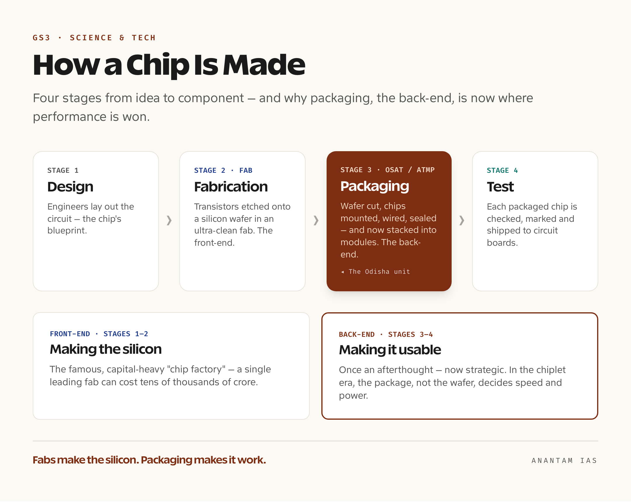
To see why this unit matters, you have to know how a chip is actually made — and where packaging fits. The journey runs in four broad stages. It starts with design, where engineers lay out the circuit. Then comes fabrication, the front-end, carried out in a “fab” — a fabrication plant, the ultra-clean factory where transistors are etched onto a polished disc of silicon called a wafer, layer by microscopic layer. This is the glamorous, capital-heavy part everyone pictures when they hear “chip factory.” A leading fab can cost tens of thousands of crore.
But a finished wafer is useless on its own. It has to be cut into individual chips, mounted, wired up, sealed in a protective body and tested before it can sit on a circuit board. That back-end work is packaging and testing, and the industry has a clumsy acronym for the firms that do it: OSAT, for Outsourced Semiconductor Assembly and Test. In India the same activity is usually written as ATMP — Assembly, Testing, Marking and Packaging. Packaging is what protects the fragile silicon, connects its tiny internal wiring to the outside world, manages heat, and gives the chip the body you can actually handle. For decades this was treated as low-value grunt work, done far from the prestigious fabs. So packaging and fabrication are two halves of one whole: fabs make the silicon, OSAT/ATMP units make it usable.
That hierarchy has flipped, and the reason is the chiplet era. For half a century, progress meant cramming ever more transistors onto a single slab of silicon — the famous Moore’s Law. But shrinking transistors has become brutally hard and expensive, and a single giant chip is costly to make because one tiny defect can ruin the whole thing. So designers switched strategy. Instead of one big chip, they now build several smaller specialist chips — called chiplets — and stitch them together inside a single package: a fast logic chiplet next to a block of memory next to an input-output piece, each made on whatever process suits it best. The package, not the wafer, becomes the place where the system comes together. This is advanced packaging, and heterogeneous integration is its formal name — “heterogeneous” simply meaning you mix different chip types in one package. When you stack them vertically rather than laying them flat, you get 3D packaging. Suddenly the back-end is where performance is won or lost, which is exactly why a packaging unit, not just a fab, is strategic.
The Project and the Glass-Substrate Technology
So what exactly is being built at Info Valley, and why glass? Start with the substrate — the base plate a chip is mounted on, which carries the wiring that links the chip to the outside circuit board. Traditionally this plate is made of an organic resin (think reinforced plastic) or, for high-end work, silicon. The unit in Odisha will use glass instead, and that swap is the whole point.
Glass has properties that the chiplet era prizes. It stays flat and rigid under heat instead of warping, which lets engineers build bigger, denser packages without the plate buckling. Its electrical behaviour is cleaner — a lower dielectric constant, in the jargon — so signals travel between stacked chips faster and with less energy wasted as heat, which matters enormously at the very high frequencies used in artificial-intelligence accelerators and 5G or 6G gear. And it allows finer, denser wiring than organic substrates can. As the project’s backers describe it, 3D Glass Solutions brings a proprietary glass-ceramic packaging platform protected by over a hundred patents, while Intel — itself a leading developer of glass-substrate research — contributes process and technology support. So this is not a copy of an existing Indian line; it’s an attempt to start near the frontier.
The numbers, as announced, give a sense of scale. The plant targets about 70,000 glass panels and 50 million assembled units a year, plus roughly 13,000 high-end 3DHI modules. The total cost is around ₹1,943 crore — split between ₹799 crore of central support through the India Semiconductor Mission and close to ₹400 crore from Odisha, with the promoter funding the rest. Commercial production is slated for August 2028 and full capacity for 2030. The chips it packages are aimed at high-performance computing, AI, data centres, telecom and defence and aerospace electronics — precisely the sectors where India most wants to reduce import dependence. And the location is not random: Info Valley already hosts SiCSem, India’s first commercial compound-semiconductor fab, so Odisha becomes the first state to pair a fab and an advanced packaging line in one cluster.
Significance for India’s Chip Mission
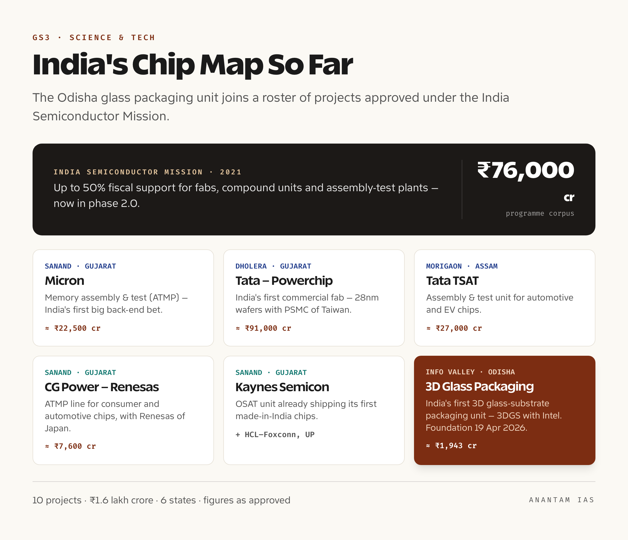
This unit is one piece of a deliberate national strategy, and that’s where its real weight lies. India launched the India Semiconductor Mission (ISM) in 2021 with a corpus of about ₹76,000 crore — formally the Modified Programme for semiconductors and display manufacturing. The idea was to offer generous fiscal support, up to 50 per cent of project cost, to anyone willing to set up fabs, compound-semiconductor units, display fabs, or assembly-and-test (ATMP/OSAT) plants on Indian soil, alongside a separate design-linked incentive for chip designers. The goal is blunt: build the missing factories so India isn’t wholly dependent on imported chips for everything from phones to missiles.
The Odisha packaging unit slots into the back-end leg of that plan, and it joins a roster that has filled out fast. By late 2025 the mission had cleared ten projects worth roughly ₹1.6 lakh crore across six states. The marquee names are worth knowing. Micron is building a memory ATMP plant at Sanand in Gujarat, the country’s first big assembly-and-test investment. Tata Electronics, with Taiwan’s Powerchip (PSMC), is building India’s first commercial fab at Dholera in Gujarat — a roughly ₹91,000-crore project meant to make wafers at the 28-nanometre node. Tata’s TSAT is putting up an assembly-and-test unit at Morigaon in Assam. CG Power, with Japan’s Renesas and a Thai partner, is building an ATMP line at Sanand; Kaynes Semicon has its own OSAT unit at Sanand that has already begun shipping chips; and an HCL-Foxconn venture in Uttar Pradesh will package display-driver chips. The Odisha glass unit adds the most advanced packaging node to that mix.
And there’s a sequel. In the Union Budget for 2026-27 the government announced ISM 2.0, the mission’s next phase, with a fresh allocation to seed it. Where ISM 1.0 was about attracting the first factories, ISM 2.0 leans toward deeper goals — making the equipment and materials that fabs themselves need, building home-grown intellectual property and design strength, and hardening the supply chain so India isn’t merely assembling other people’s technology. The stated targets are ambitious: meeting 70-75 per cent of domestic chip demand by 2029 and reaching the most advanced manufacturing in the years after. Against that backdrop the Odisha unit is a marker of how the mission is maturing — from “can we make chips at all” toward “can we own the most valuable, hardest parts of the process.” Owning advanced packaging is exactly that kind of high-value capability, and it directly serves the wider push for self-reliance and supply-chain resilience that runs through India’s whole technology policy.
Challenges and the Way Forward
None of this is guaranteed, and a balanced view has to name the hurdles. The first is execution risk and time. The plant won’t make commercial product until 2028 and won’t hit full scale until 2030, and semiconductor projects worldwide are notorious for slipping. Frontier glass-substrate manufacturing is so new that even the biggest firms are still ironing out yields — making complex parts reliably, without too many duds — so a first-of-its-kind line in a country new to the field faces a steep learning curve.
The second is the ecosystem around the factory. A packaging plant needs ultra-pure chemicals and gases, specialised materials, precision equipment and a steady supply of trained technicians and engineers — most of which India still imports or lacks. Build the box without the supply chain and skilled people to run it, and the plant stays dependent on the very imports it was meant to reduce. That’s precisely why ISM 2.0’s focus on materials, equipment and skilling matters, and why states like Odisha are amending their semiconductor policies to fund parks, training and R&D rather than just handing out capital subsidies. Add the sheer capital intensity and the fact that India is entering a market dominated by entrenched giants in Taiwan, South Korea and the US, and the scale of the climb is clear.
So what’s the way forward? Steady policy and patient capital, first of all — the incentives have to outlast political cycles, because payback in this industry takes a decade. Deep investment in talent through specialised courses and tie-ups with global firms, so the plants have people to staff them. A determined effort to build the supplier base — the chemicals, gases and tool-makers — at home, which is exactly ISM 2.0’s brief. And realistic expectations: India is starting at mature and back-end nodes, not at the bleeding edge of the smallest transistors, and that’s the sensible place to begin. Get those pieces right, and the Odisha glass unit could be remembered as the moment India moved from making chips to mastering the part of the chain where the next decade’s value will sit. Get them wrong, and it risks being an expensive island. The foundation stone is laid; the harder building starts now.
For Your Mains Answer
This is a high-value topic for GS Paper 3, which covers science and technology developments, indigenisation of technology, the economy and infrastructure. It maps cleanly onto questions on India’s semiconductor strategy, achievements in science and tech, self-reliance (Aatmanirbhar Bharat), and supply-chain or economic-security themes. It can also feed an Essay on technological sovereignty. The skill that scores is the same one this article uses: explain the technology in plain terms, then place a single project inside the national mission and the global trend, and end with a measured verdict.
How to Build the Answer
Move along the value chain. Open by defining the two halves of chipmaking — fabrication (front-end, in a fab) and packaging (back-end, OSAT/ATMP) — and explain why packaging has become strategic in the chiplet era. Then introduce the Odisha unit: the company (3D Glass Solutions through HIPSPL, with Intel), the technology (3D heterogeneous integration on glass substrates), the outlay (₹1,943 crore) and the date (19 April 2026). Next, zoom out to the India Semiconductor Mission — the ₹76,000-crore scheme, the ten approved projects, ISM 2.0 — and the global de-risking trend. Close with a balanced judgement on execution, ecosystem and skills. That arc — define, locate, contextualise, evaluate — fits almost any semiconductor question.
Common Mistakes to Avoid
Don’t treat “semiconductor manufacturing” as one thing — examiners reward candidates who separate fabrication from packaging. Don’t confuse a fab with an ATMP/OSAT unit; this Odisha project is packaging, not a fab. Don’t overstate the achievement as “India now makes its own advanced chips” — it packages them, and only from 2028. And don’t forget the qualifier “as announced” on figures and timelines, since first-of-a-kind projects often slip.
A Compact Answer Spine
Chipmaking = front-end fabrication (fab, etches transistors on wafers) + back-end packaging/testing (OSAT/ATMP) → chiplet era makes packaging strategic → 19 Apr 2026: India’s first 3D glass packaging unit at Info Valley, Bhubaneswar, by 3D Glass Solutions/HIPSPL with Intel, ₹1,943 cr (ISM ₹799 cr + Odisha ₹400 cr), output from 2028 → fits ISM (₹76,000 cr, 2021) and ISM 2.0; joins Micron, Tata-PSMC Dholera, Tata Morigaon, CG-Renesas, Kaynes, HCL-Foxconn → significance: back-end self-reliance, supply-chain resilience → challenges: execution, ecosystem, skills, capital → verdict: a maturing, high-value bet, not yet a finished capability.
Diagram or Flowchart Idea
Draw a simple left-to-right chain — Design → Fabrication (fab) → Packaging/Assembly (OSAT/ATMP) → Test — with the packaging box circled and labelled “where India’s Odisha unit fits.” Beside it, a small stack of three labelled chiplets (logic, memory, I/O) sitting on a glass plate captures heterogeneous integration at a glance. A clean two-part visual like this communicates the whole story fast and is quick to sketch.
A Balanced-Conclusion Line
A line that lands the marks: “India’s first glass packaging unit is less a finished triumph than a strategic down-payment — staking a claim in the part of chipmaking where tomorrow’s value lies, even as the harder work of building an ecosystem, a skilled workforce and reliable yields has only begun.”
How to Use Data Without Cramming
You need four anchors, not a spreadsheet: 19 April 2026 (the groundbreaking), ₹1,943 crore (the outlay), ₹76,000 crore (the ISM corpus), and ten approved projects across six states. Drop those into the right sentences and attribute them plainly — “as the government announced” — and the answer reads as authoritative without a wall of numbers.
FAQ
What exactly is being built in Odisha, and who is building it? India’s first advanced 3D glass semiconductor packaging unit, at Info Valley in Bhubaneswar. It will stack and connect multiple chips vertically (3D heterogeneous integration) on glass-core substrates rather than the usual plastic or silicon. The promoter is Heterogeneous Integration Packaging Solutions Pvt Ltd, the Indian subsidiary of US firm 3D Glass Solutions, with Intel providing technology and process expertise. The foundation stone was laid on 19 April 2026, with commercial production targeted for August 2028 and full scale by 2030.
How is packaging different from a chip fab? A fab (fabrication plant) is the front-end: it etches transistors onto silicon wafers, the part most people picture as “making chips.” Packaging is the back-end: it cuts the wafer into chips, mounts and wires them, seals and tests them, and increasingly stacks several chips into one module. The industry calls back-end firms OSAT (Outsourced Semiconductor Assembly and Test); in India the activity is often labelled ATMP (Assembly, Testing, Marking, Packaging). The Odisha unit is a packaging facility, not a fab.
Why does advanced packaging matter so much now? Because of the chiplet era. Shrinking transistors on a single chip has hit physical and cost limits, so designers now combine several smaller specialist chips — chiplets — inside one package. The package, not the wafer, is where performance is now won, making advanced packaging strategically vital. Glass substrates push this further by allowing faster, denser, cooler connections between stacked chips — useful for AI, 5G/6G and defence electronics.
How does this fit the India Semiconductor Mission? The India Semiconductor Mission, launched in 2021 with about ₹76,000 crore, offers up to 50 per cent fiscal support for fabs, compound-semiconductor units, display fabs and assembly-and-test plants. The Odisha unit gets ₹799 crore of central support through the mission, plus state funding. It joins ten approved projects worth roughly ₹1.6 lakh crore — including Micron, Tata-PSMC Dholera, Tata Morigaon, CG Power-Renesas, Kaynes and HCL-Foxconn — and complements ISM 2.0, the mission’s deeper next phase announced in the 2026-27 Budget.
Practice Questions
Prelims MCQs
- The advanced semiconductor unit whose foundation was laid in Odisha in April 2026 is primarily concerned with which stage of chipmaking?
(a) Chip design
(b) Wafer fabrication in a fab
(c) Advanced packaging and assembly
(d) Raw silicon refining
Answer: (c) The Info Valley unit is a 3D glass packaging and assembly facility — the back-end (OSAT/ATMP) stage — not a fabrication plant. - With reference to “OSAT” and “ATMP” in the semiconductor industry, which statement is correct?
(a) They refer to the design of new chips
(b) They refer to the assembly, testing and packaging of chips (the back-end)
(c) They refer to the manufacture of silicon wafers
(d) They are names of government subsidy schemes
Answer: (b) OSAT (Outsourced Semiconductor Assembly and Test) and ATMP (Assembly, Testing, Marking, Packaging) both describe the back-end packaging and testing of chips. - Why is glass being used as a substrate material in the Odisha packaging unit?
(a) It is cheaper than every other material in all uses
(b) It stays flat under heat, has cleaner electrical behaviour and allows denser, faster connections
(c) It is the only material that can etch transistors
(d) International rules now ban organic substrates
Answer: (b) Glass resists warping under heat, has a lower dielectric constant for faster, lower-loss signals, and allows finer, denser wiring than organic substrates — useful for AI and high-frequency chips. - The India Semiconductor Mission, under which the Odisha unit receives central support, is associated with which of the following?
(a) A corpus of about ₹76,000 crore and up to 50 per cent fiscal support
(b) Full government ownership of all approved fabs
(c) A ban on importing any semiconductors
(d) Support only for chip design, not manufacturing
Answer: (a) The mission, launched in 2021, offers up to 50 per cent fiscal support to fabs, compound-semiconductor units, display fabs and assembly-and-test plants under a roughly ₹76,000-crore programme. - Which of the following correctly pairs an approved Indian semiconductor project with its location?
(a) Micron ATMP — Dholera
(b) Tata-Powerchip fab — Sanand
(c) CG Power-Renesas ATMP — Sanand
(d) HCL-Foxconn packaging — Morigaon
Answer: (c) CG Power, with Renesas, is building an ATMP unit at Sanand, Gujarat. Micron’s ATMP is at Sanand, the Tata-Powerchip fab is at Dholera, and HCL-Foxconn’s unit is in Uttar Pradesh.
Mains Practice Questions
- Distinguish between semiconductor fabrication and packaging, and explain why advanced packaging has become strategically important in the “chiplet era.” (15 marks, 250 words)
- “India’s first 3D glass semiconductor packaging unit is a strategic down-payment rather than a finished capability.” Critically examine this statement in the context of the India Semiconductor Mission. (15 marks, 250 words)
- Discuss the architecture and objectives of the India Semiconductor Mission, and assess how its approved projects address different stages of the semiconductor value chain. (15 marks, 250 words)
- How does owning back-end packaging capability contribute to India’s goals of self-reliance and supply-chain resilience in critical technologies? (10 marks, 150 words)
- Examine the key challenges India faces in building a domestic semiconductor ecosystem, and suggest a way forward in light of ISM 2.0. (15 marks, 250 words)
Tell Google you want more of this.
Add Anantam IAS as a preferred sourceOne tap, and this site shows up more often in your own Top Stories, AI Overviews and AI Mode. Remove it any time.