Opens in a new tab
Join Anantam IAS Channel on Telegram

Daily Digest · Tuesday

7 April 2026 Current Affairs for UPSC

2 current affairs published on Tuesday, 7 April 2026

7 April 2026 Current Affairs for UPSC — every Why-in-News article AnantamIAS published on Tuesday, 7 April 2026, broken down with Why in News?, the exact GS paper it feeds, sub-topic mapping, MCQ-ready facts and a UPSC-style practice question. 2 articles in total, covering Polity, Economy, Environment, S&T, IR, Geography, History, Society and Internal Security — the same Why-in-News + GS-paper-mapping + practice-question format the Compass uses across every daily digest on the site.

Daily current affairs for UPSC is where new material enters your prep stream. Read this 7 April 2026 digest end-to-end in 25–35 minutes, attempt the practice question at the foot of each article (it's MCQ for some, 10/15-marker for others), then bookmark the entries that fall inside your active revision window. Everything stays cross-linked: tap any subject pill to jump to that subject's hub, or use the table of contents above to skip straight to a specific story.

Use this page three ways. Read sequentially for a one-sitting scan of everything that mattered on 7 April 2026. Download the 7 April 2026 PDF below for offline study or print revision. Or use the April 2026 Current Affairs compilation to see this day in the month's full context. For the previous day's reading, see 6 April 2026 Current Affairs; the next day's is 8 April 2026 Current Affairs.

Why we publish daily current affairs separately from the monthly compilation: daily is learning, monthly is revision. Use the daily page to add fresh material to your notes the day it breaks; come back to the April 2026 compilation 60 days before Prelims when the noise has settled and only the lasting takeaway is worth re-reading.

Kalpakkam Fast Breeder Reactor attains Criticality

Open article →Download PDF

Why in News?

India’s prototype fast-breeder reactor (PFBR) in Tamil Nadu’s Kalpakkam (500 MWe) has successfully achieved first criticality (the start of a controlled fission chain reaction).

UPSC Relevance: GS-3 Science and Technology: Nuclear Technology

Prelims: Key concepts associated with Nuclear Technology;
Mains: India’s Three-Stage Nuclear Programme; Fast Breeder Reactor

 Key concepts associated with Nuclear Technology:

Back to Basics: Key Concepts
Natural Uranium:
• Natural Uranium is composed of three major isotopes:
Uranium-238 (99.284% natural abundance)
Uranium-235 (0.711%)
Uranium-234 (0.005%) 

• U-235 atoms are the only nuclide existing in nature (in appreciable amounts) that is fissile with thermal neutrons. Hence, Uranium enrichment is necessary to create a high enough concentration of U-235 out of mined Uranium. 
Nuclear Fuel (Fertile vs Fissile):
• Fissile Material: Fissile isotopes readily undergo fission when hit by neutrons. E.g., Uranium-235 (U-235), Uranium-233 (U-233) and Plutonium-239 (Pu-239). 

• Fertile Material: Fertile isotopes are not directly fissile by slow neutrons. However, fertile isotopes can absorb neutrons and transmute into fissile materials through radioactive decay. E.g., Uranium-238 (U-238); Thorium-232 (Th-232). 
Nuclear Transmutation:
• Refers to the conversion of one nuclide into another within the fuel or target material. This process can involve the absorption of a neutron, the emission of a neutron, or the capture and subsequent decay of a particle.
Criticality of Nuclear Reactor:
• Criticality in a nuclear reactor is the point at which the nuclear chain reaction becomes self-sustaining. ​​
• A nuclear reactor is said to be critical when the number of neutrons produced in Nuclear fission reactions equals the number of neutrons lost through absorption, leakage, and other processes. This equilibrium state allows for a sustained and controlled chain reaction.
Pressurised Heavy Water Reactors (PHWRs):
• PHWRs commonly use unenriched natural uranium as their fuel and heavy water (deuterium oxide, D2O) as both coolant and moderator.
• Control Rods: Boron or cadmium control rods are used to absorb excess neutrons and regulate the nuclear reaction.
• Advantages: PHWRs use natural uranium fuel, produce less high-level radioactive waste, and operate at lower pressures compared to some other reactor types.
Fast Breeder Reactor (FBR):
• A breeder reactor is a nuclear reactor that produces more fissile material than it consumes. 
• FBR uses fast neutrons (without a moderator) to convert fertile material into fissile fuel, thereby “breeding” additional nuclear fuel.
• Fuelled by: Mixed Oxide (MoX) Fuel. It generally contains 3%-5% Plutonium Oxide blended with 95-97% natural or depleted Uranium Oxide. It uses liquid sodium as a coolant.

Prototype Fast Breeder Reactor (PFBR), Kalpakkam: 

• India’s first 500 MWe nuclear reactor. Located at Kalpakkam, Tamil Nadu.
• Being implemented by Bharatiya Nabhikiya Vidyut Nigam Limited (BHAVINI), a public sector enterprise under India’s Department of Atomic Energy (DAE). 
• Fuelled by: Mixed Oxide (MoX) Fuel. It generally contains 3%-5% Plutonium Oxide blended with 95-97% natural or depleted Uranium Oxide. It uses liquid sodium as a coolant.
• Operational Timeline: scheduled for full power generation by late 2026.
The reactor has been fully designed and constructed indigenously by BHAVINI and the Indira Gandhi Centre for Atomic Research (IGCAR). 
• Significance: PFBR is central to 2nd Stage of India’s three-stage nuclear power programme.
image 23 1

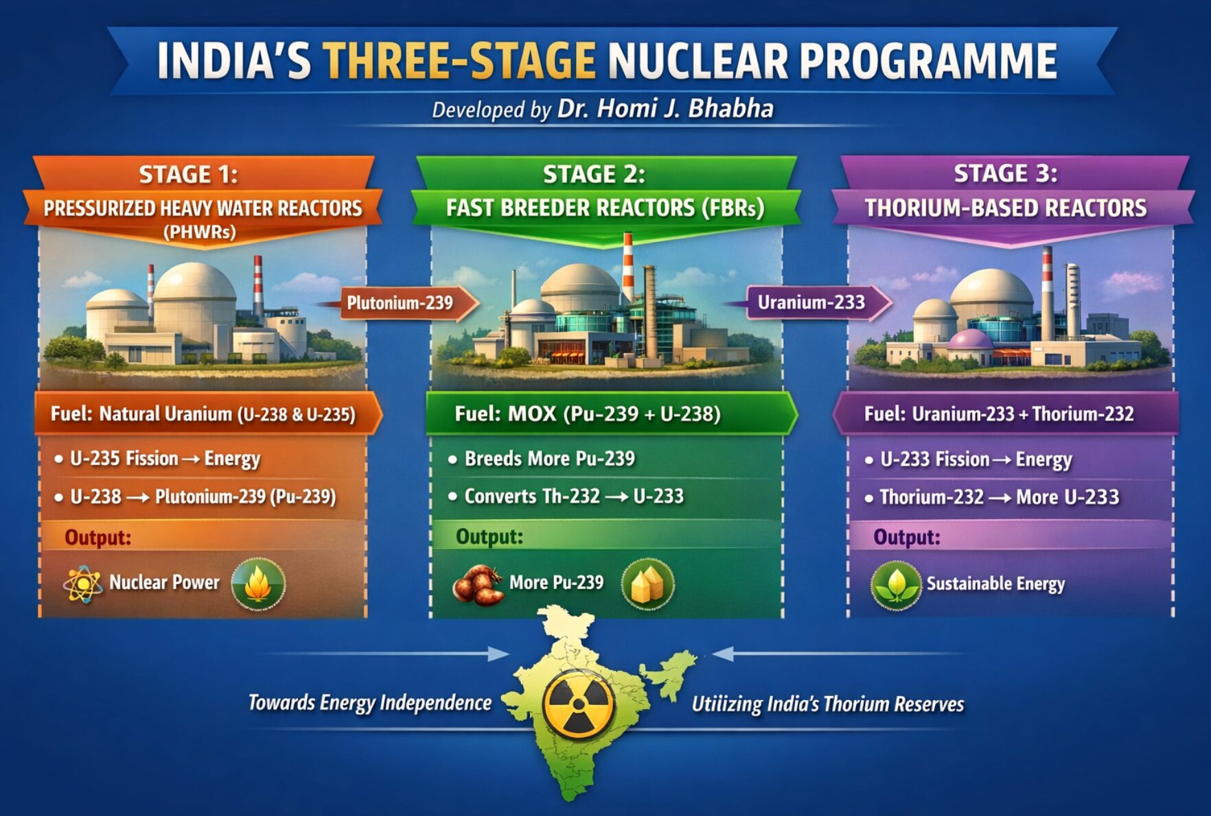
India’s Three-Stage Nuclear Programme: 

  • The three-stage nuclear programme of India was formulated by Dr Homi J. Bhabha.
  • Aim: It is a long-term strategy designed to make the country self-reliant in nuclear energy, especially using its abundant thorium reserves.
  • Need: India lacks large uranium reserves but has vast thorium deposits. So, the programme is structured to:
    • Use limited uranium efficiently.
    • Gradually shift to thorium-based energy.
Thorium Reserves of India:
• India has about 25% of the global thorium in the form of monazite sands along its coastline.
• Distribution: Coastal and inland placer sands on the beaches of Kerala, Tamil Nadu, Odisha, Andhra Pradesh, Maharashtra, and Gujarat, and inland riverine sands of Jharkhand and West Bengal.  

First Stage: Pressurised Heavy Water Reactors (PHWRs)

  • The first stage includes the setting up of Pressurised Heavy Water Reactors.
  • Fuel used: Natural Uranium (99.3% U-238 and 0.7% U-235)
  • Process:
    • U-235 undergoes fission and produces energy.
    • U-238 absorbs neutrons and gets converted into Plutonium-239 (Pu-239). 
  • Outcome: Generation of Nuclear Energy & production of Plutonium for the next stage. 

Second Stage: Fast Breeder Reactor (FBR)

  • Fuel used: Uranium-Plutonium Mixed Oxide (MOX) fuel. It is a mix of Plutonium-239 (byproduct/radioactive waste produced in the 1st stage) and Uranium-238. 
  • Process: 
    • Pu-239 is used as the fuel core. The surrounding blanket of U-238 absorbs neutrons to produce more fuel (Pu-239). Since the amount of Plutonium produced inside the reactor is more than that initially used, it is called a breeder reactor. 
    • Begins conversion of thorium (Th-232) into fissile uranium-233 (U-233) that will be used in the 3rd stage.
  • The reactor uses fast neutrons without the need for a moderator to slow them down. Fast neutrons are more efficient at inducing fission in certain isotopes (such as Plutonium-239). 
  • Outcome: Breeds more fuel (Pu-239) than it consumes. Prepares U-233 for stage 3. 
Significance of Fast Breeder Reactor:

• Closed fuel cycle: Significant reduction in nuclear waste generated as FBR utilises (reprocesses) the radioactive waste (Plutonium-239) from the 1st stage as fuel in the 2nd stage.  

• Energy independence: Act as a critical link between uranium and thorium fuel cycles. Stepping stone for the 3rd stage of India’s Nuclear Programme. 

• Advanced safety features: Advanced reactor with inherent passive safety features, which enable automatic reactor shutdown in case of abnormal conditions. 

• Economic viability: Both the capital cost and the per-unit electricity cost are comparable to those of other nuclear and conventional power plants. 

Third Stage: Thorium-Based Reactors 

  • Fuel used: Uranium-233 + Thorium-232
  • Process:
    • U-233 undergoes fission.
    • Thorium-232 converts into more U-233. 
  • Outcome: Sustainable nuclear energy using India’s thorium reserves. 

This is a landmark achievement for India’s nuclear energy programme, marking a historic step in providing long-term energy security and advancing indigenous nuclear technology capabilities.

UPSC PYQ 2023

Q. Consider the following statements:

Statement I: India, despite having uranium deposits, depends on coal for most of its electricity production.

Statement II: Uranium, enriched to the extent of at least 60%, is required for the production of electricity.

Which one of the following is correct with respect to the above statements?

(a) Both Statement I and Statement II are correct, and Statement II is the correct explanation for Statement I

(b) Both Statement-I and Statement-II are correct, and Statement-II is not the correct explanation for Statement-I

(c) Statement I is correct, but Statement II is incorrect

(d) Statement I is incorrect, but Statement II is correct

Answer: (c) 

UPSC PYQ 2016

Q. India is an important member of the ‘International Thermonuclear Experimental Reactor’. If this experiment succeeds, what is the immediate advantage for India?

(a) It can use thorium in place of uranium for power generation

(b) It can attain a global role in satellite navigation

(c) It can drastically improve the efficiency of its fission reactors in power generation

(d) It can build fusion reactors for power generation

Answer: (d) 

UPSC Mains PYQ 2018

Q. With growing energy needs, should India keep on expanding its nuclear energy programme? Discuss the facts and fears associated with nuclear energy.

UPSC Mains PYQ 2017

Q. Give an account of the growth and development of nuclear science and technology in India. What is the advantage of the fast breeder reactor programme in India? 
India’s Semiconductor Mission: Policy Push & Challenges 

Open article →Download PDF

Why in News?

Recently, the Prime Minister of India inaugurated the ₹3,300 crore Kaynes Technology semiconductor Outsourced Semiconductor Assembly and Test (OSAT) facility in Sanand, Gujarat. The project is hailed as a major boost to the domestic chip manufacturing ecosystem.

UPSC Relevance: GS-3 Economy: Manufacturing; Science and Technology: Frontier Technology

Prelims: Semicon India Programme; Pax Silica Initiative; iCET
Mains: Semiconductors: Role in economic growth & challenges associated

With the leap forward towards digitalisation and automation, semiconductors have become integral to economic security and strategic independence. They power essential systems in healthcare, transport, communication, defence, and space. 

Semicon India Programme: 

  • A strategic initiative launched in 2021 aimed to establish a robust semiconductor and display manufacturing ecosystem in India. It seeks to position India as a global hub for electronics manufacturing and chip design.
  • Objective: To reduce import dependence and position India as a global hub for electronics manufacturing and chip design.
  • Outlay: about ₹76,000 crore
  • Implementing agency: India Semiconductor Mission (ISM), a nodal agency set up under the Ministry of Electronics and Information Technology (MeitY).
  • Focus areas: 
    • Semiconductor fabs (chip manufacturing units)
    • Display fabs
    • Chip design ecosystem
    • Packaging & testing units
    • R&D and talent development
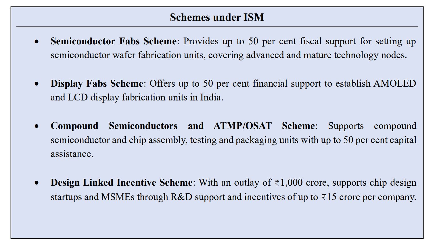
  • Financial incentives up to 50% of the project cost are provided to companies involved in Semiconductor Fabs, Display Fabs, Assembly, Testing, Marking, and Packaging (ATMP/OSAT) units, and Semiconductor Design.
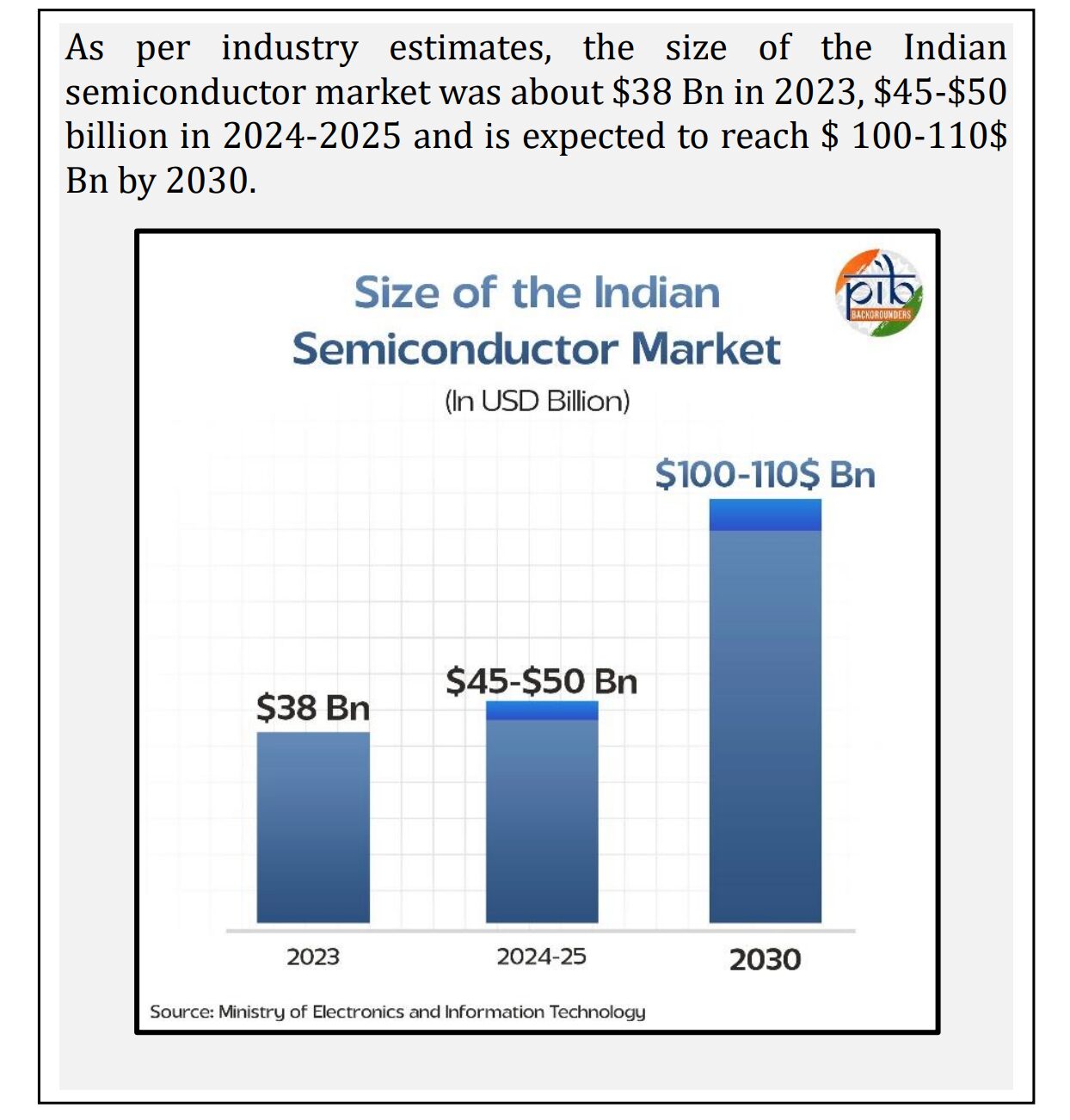
image 24 1

    About Semiconductors:

    About Semiconductors: 
    • Definition: Materials with electrical conductivity between those of conductors (e.g., metals) and insulators (e.g., rubber).
    • Semiconductors are made from pure elements, typically silicon or germanium, or compounds such as gallium arsenide. They are sometimes referred to as integrated circuits (ICs) or microchips. 
    • Their electrical properties can be modified through a process called doping, where small amounts of impurities are added to these pure elements, allowing them to conduct electricity more efficiently. E.g., Silicon Carbide
    • Key Components: Diodes, transistors, microchips, photovoltaic cells, LEDs, and mounted piezo-electric crystals.

    • Applications: 
    ‣ Electronics: Foundational components in computers, smartphones, and LEDs.
    ‣ Renewable Energy: Used in solar cells.
    ‣ Defence and Space: Integral to missile guidance systems and satellite communication.
    image 25

    Government efforts to boost Semiconductor Production:

    1. Manufacturing Facilities under the Semicon India Programme:

    • The Indian government has approved 12 major semiconductor manufacturing projects (encompassing silicon fabs, compound semiconductors, and packaging units) alongside 24 chip design projects.
    • These would cater to chip requirements of sectors such as consumer appliances, industrial electronics, automobiles, telecommunications, aerospace, and power electronics, etc. 

    2. Relaxation of SEZ Rules to Promote Semiconductor Manufacturing:

    To further encourage the domestic manufacturing of semiconductors and electronic components, the government has relaxed the key provisions of the SEZ Rules, 2006:

    • Reduction in Minimum Land Requirement: Earlier, SEZs exclusively for semiconductor/electronics manufacturing required a minimum of 50 hectares of contiguous land. The requirement has now been reduced to 10 hectares, lowering entry barriers and investment costs.
    • Relaxation in Encumbrance-free Land Requirement: Earlier, land for SEZs had to be completely free from legal or financial encumbrances. The Board of Approval (BoA) can now relax this condition where land is mortgaged or leased to Central/State Governments or their agencies.
    • Permission for Domestic Sales: Conventionally, SEZs are exclusively export-oriented. SEZ units in semiconductor and electronics manufacturing are now allowed to sell in the Domestic Tariff Area (DTA) after paying applicable duties.

    3. India Semiconductor Mission 2.0:

    • The Union Budget 2026-27 allocated Rs 1000 crores for the India Semiconductor Mission 2.0. 
    • ISM 2.0 will focus on:
      • advanced manufacturing to achieve 3-nanometre and 2-nanometre technology nodes. 
      • designing full-stack Indian semiconductor intellectual property.
      • strong emphasis on industry-led research and training centres to drive technology development and create a future-ready skilled workforce.

    4. International Partnerships:

    • India-USA Semiconductor Partnership operates under the framework of the India-U.S. Initiative on Critical and Emerging Technology (iCET) launched in 2023.
    • Industrial Collaboration with Taiwan, South Korea, Japan, and the EU to build a resilient supply chain, attract investment, access advanced technology and integrate into global value chains.
    • India formally joined the Pax Silica coalition in 2026.
    Pax Silica Initiative: 
    • Pax Silica is a U.S.-led strategic initiative to build a secure, prosperous, and innovation-driven silicon supply chain. 
    • Aim: To reduce overconcentration in global supply chains, prevent economic coercion, and ensure that emerging technologies are developed and governed by open, democratic societies. It seeks to secure AI and semiconductor supply chains.
    • Key signatory nations: United States, India, Japan, South Korea, Singapore, Australia, Israel, the United Kingdom, Qatar, and the UAE. 

    Associated Challenges: 

    • Capital-intensive and longer gestation period: Setting up a semiconductor fabrication unit can cost $5-20 billion, depending on node technology. A long gestation period carries the risk of technology becoming obsolete before investment recovery. Thus, the units require sustained funding support from the government.
    • Structural constraint: FDI in electronics is less than 1% of the total FDI inflow because of the dearth of skilled labour, delays in land acquisition, and the uncertain tax regime.
    • Infrastructure Constraints: Semiconductor fabs require:
      • uninterrupted electricity (24*7 power supply & zero fluctuation)
      • ultra-pure water in large quantities
      • efficient logistics and proximity to airports
    • Technology Gap in Advanced Nodes: Current Indian fabrication units mainly focus on mature nodes (28nm or above). Advanced chip manufacturing (5nm, 3nm, etc.) is dominated by Taiwan, South Korea, USA.
    • Technological Constraints: Indigenous advanced manufacturing requires high-end technologies which licensed from patent holders at a very high price. 
    • Underdeveloped Semiconductor Supply Chain: Dependence on imports for silicon wafers, speciality gases, photolithography equipment & rare earth minerals. This makes the sector vulnerable to supply chain disruption. 

    India Semiconductor Mission focuses on design, manufacturing, and packaging. India Semiconductor Mission 2.0 will expand beyond the first phase to include materials, research and development, chemicals, gases, equipment manufacturing, and skilling.