
Why in News?
Recently, the Prime Minister of India inaugurated the ₹3,300 crore Kaynes Technology semiconductor Outsourced Semiconductor Assembly and Test (OSAT) facility in Sanand, Gujarat. The project is hailed as a major boost to the domestic chip manufacturing ecosystem.
| UPSC Relevance: GS-3 Economy: Manufacturing; Science and Technology: Frontier Technology Prelims: Semicon India Programme; Pax Silica Initiative; iCET Mains: Semiconductors: Role in economic growth & challenges associated |
With the leap forward towards digitalisation and automation, semiconductors have become integral to economic security and strategic independence. They power essential systems in healthcare, transport, communication, defence, and space.
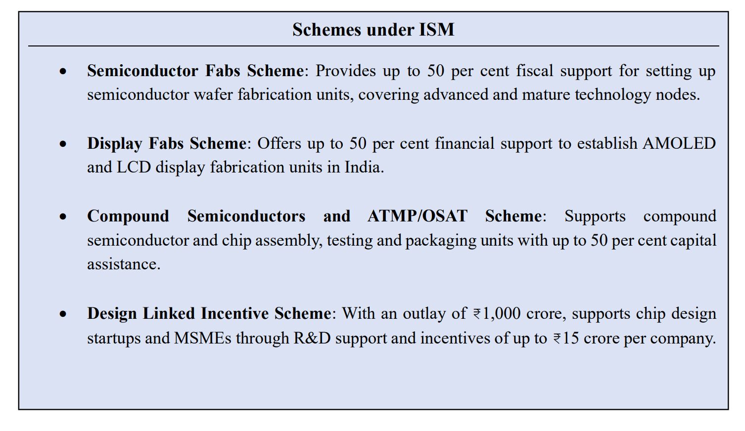
Semicon India Programme:
- A strategic initiative launched in 2021 aimed to establish a robust semiconductor and display manufacturing ecosystem in India. It seeks to position India as a global hub for electronics manufacturing and chip design.
- Objective: To reduce import dependence and position India as a global hub for electronics manufacturing and chip design.
- Outlay: about ₹76,000 crore
- Implementing agency: India Semiconductor Mission (ISM), a nodal agency set up under the Ministry of Electronics and Information Technology (MeitY).
- Focus areas:
- Semiconductor fabs (chip manufacturing units)
- Display fabs
- Chip design ecosystem
- Packaging & testing units
- R&D and talent development
- Financial incentives up to 50% of the project cost are provided to companies involved in Semiconductor Fabs, Display Fabs, Assembly, Testing, Marking, and Packaging (ATMP/OSAT) units, and Semiconductor Design.
About Semiconductors:
| About Semiconductors: • Definition: Materials with electrical conductivity between those of conductors (e.g., metals) and insulators (e.g., rubber). • Semiconductors are made from pure elements, typically silicon or germanium, or compounds such as gallium arsenide. They are sometimes referred to as integrated circuits (ICs) or microchips. • Their electrical properties can be modified through a process called doping, where small amounts of impurities are added to these pure elements, allowing them to conduct electricity more efficiently. E.g., Silicon Carbide • Key Components: Diodes, transistors, microchips, photovoltaic cells, LEDs, and mounted piezo-electric crystals. • Applications: ‣ Electronics: Foundational components in computers, smartphones, and LEDs. ‣ Renewable Energy: Used in solar cells. ‣ Defence and Space: Integral to missile guidance systems and satellite communication. |
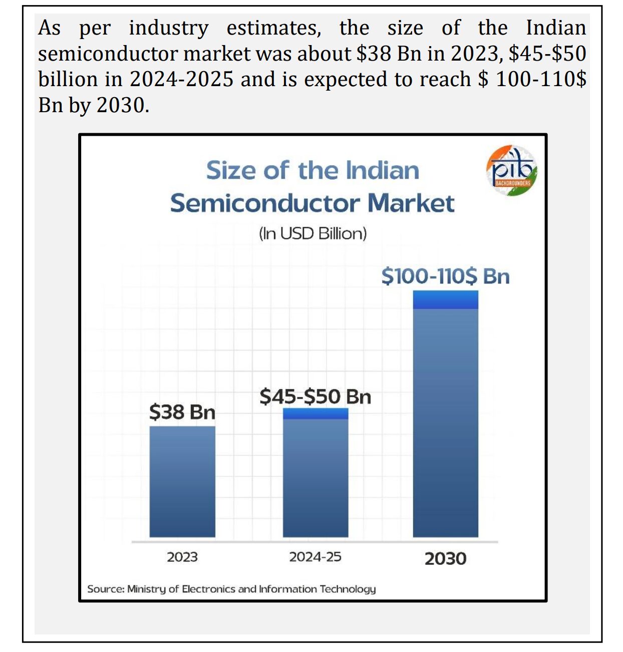
Government efforts to boost Semiconductor Production:
1. Manufacturing Facilities under the Semicon India Programme:
- The Indian government has approved 12 major semiconductor manufacturing projects (encompassing silicon fabs, compound semiconductors, and packaging units) alongside 24 chip design projects.
- These would cater to chip requirements of sectors such as consumer appliances, industrial electronics, automobiles, telecommunications, aerospace, and power electronics, etc.
2. Relaxation of SEZ Rules to Promote Semiconductor Manufacturing:
To further encourage the domestic manufacturing of semiconductors and electronic components, the government has relaxed the key provisions of the SEZ Rules, 2006:
- Reduction in Minimum Land Requirement: Earlier, SEZs exclusively for semiconductor/electronics manufacturing required a minimum of 50 hectares of contiguous land. The requirement has now been reduced to 10 hectares, lowering entry barriers and investment costs.
- Relaxation in Encumbrance-free Land Requirement: Earlier, land for SEZs had to be completely free from legal or financial encumbrances. The Board of Approval (BoA) can now relax this condition where land is mortgaged or leased to Central/State Governments or their agencies.
- Permission for Domestic Sales: Conventionally, SEZs are exclusively export-oriented. SEZ units in semiconductor and electronics manufacturing are now allowed to sell in the Domestic Tariff Area (DTA) after paying applicable duties.
3. India Semiconductor Mission 2.0:
- The Union Budget 2026-27 allocated Rs 1000 crores for the India Semiconductor Mission 2.0.
- ISM 2.0 will focus on:
- advanced manufacturing to achieve 3-nanometre and 2-nanometre technology nodes.
- designing full-stack Indian semiconductor intellectual property.
- strong emphasis on industry-led research and training centres to drive technology development and create a future-ready skilled workforce.
4. International Partnerships:
- India-USA Semiconductor Partnership operates under the framework of the India-U.S. Initiative on Critical and Emerging Technology (iCET) launched in 2023.
- Industrial Collaboration with Taiwan, South Korea, Japan, and the EU to build a resilient supply chain, attract investment, access advanced technology and integrate into global value chains.
- India formally joined the Pax Silica coalition in 2026.
| Pax Silica Initiative: • Pax Silica is a U.S.-led strategic initiative to build a secure, prosperous, and innovation-driven silicon supply chain. • Aim: To reduce overconcentration in global supply chains, prevent economic coercion, and ensure that emerging technologies are developed and governed by open, democratic societies. It seeks to secure AI and semiconductor supply chains. • Key signatory nations: United States, India, Japan, South Korea, Singapore, Australia, Israel, the United Kingdom, Qatar, and the UAE. |
Associated Challenges:
- Capital-intensive and longer gestation period: Setting up a semiconductor fabrication unit can cost $5-20 billion, depending on node technology. A long gestation period carries the risk of technology becoming obsolete before investment recovery. Thus, the units require sustained funding support from the government.
- Structural constraint: FDI in electronics is less than 1% of the total FDI inflow because of the dearth of skilled labour, delays in land acquisition, and the uncertain tax regime.
- Infrastructure Constraints: Semiconductor fabs require:
- uninterrupted electricity (24*7 power supply & zero fluctuation)
- ultra-pure water in large quantities
- efficient logistics and proximity to airports
- Technology Gap in Advanced Nodes: Current Indian fabrication units mainly focus on mature nodes (28nm or above). Advanced chip manufacturing (5nm, 3nm, etc.) is dominated by Taiwan, South Korea, USA.
- Technological Constraints: Indigenous advanced manufacturing requires high-end technologies which licensed from patent holders at a very high price.
- Underdeveloped Semiconductor Supply Chain: Dependence on imports for silicon wafers, speciality gases, photolithography equipment & rare earth minerals. This makes the sector vulnerable to supply chain disruption.
India Semiconductor Mission focuses on design, manufacturing, and packaging. India Semiconductor Mission 2.0 will expand beyond the first phase to include materials, research and development, chemicals, gases, equipment manufacturing, and skilling.
Tell Google you want more of this.
Add Anantam IAS as a preferred sourceOne tap, and this site shows up more often in your own Top Stories, AI Overviews and AI Mode. Remove it any time.