
Why in News?
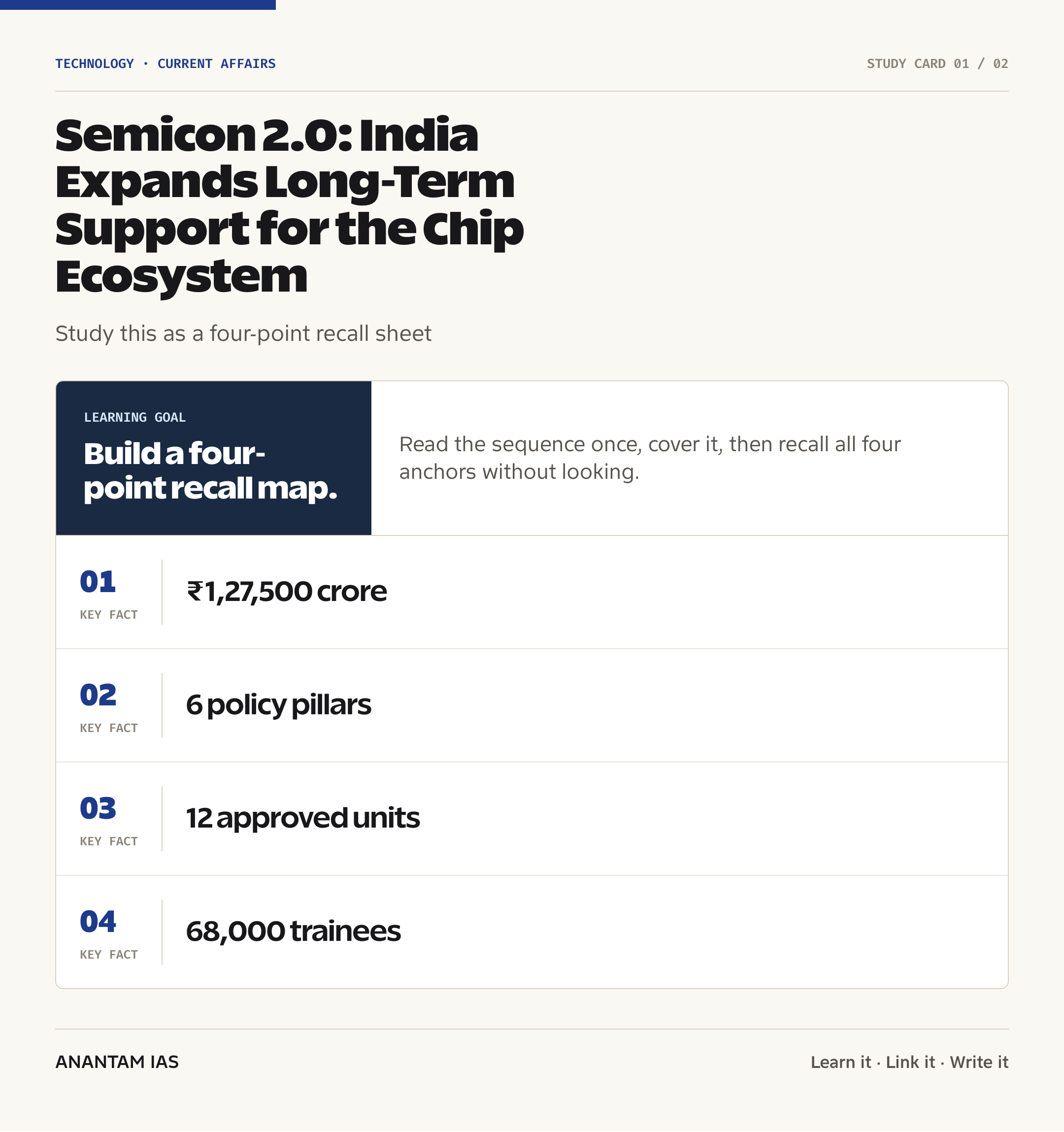
On 15 July 2026, the Union Cabinet approved Semicon 2.0 for India’s semiconductor design and manufacturing ecosystem. PIB confirmed a total budget outlay of ₹1,27,500 crore for sustained, long-term policy support.
The new phase builds on Semicon India Programme 1.0 and organizes support around six pillars: design, machines and materials, additional fabrication facilities, advanced packaging, research and development, and talent. Its central shift is from attracting isolated plants to building a complete chip ecosystem.
- The Cabinet approval covers both semiconductor design and manufacturing, rather than treating fabrication as the only policy objective.
- The first domestic semiconductor fab supported by the existing programme is scheduled for commissioning in 2028.
- Semicon 2.0 will encourage silicon fabs, compound-semiconductor fabs, discrete-component fabs and display fabs.
- The programme will deepen ATMP/OSAT capabilities and seek more advanced packaging technologies in India.
- It will support domestic production and research in equipment, materials, specialty chemicals and gases needed for chip manufacturing.
The development matters in the context of:
- The policy belongs to a wider debate on techno-nationalism: governments seek secure access to critical technologies while remaining connected to global research, equipment and markets.
- India’s challenge is not merely to assemble imported dies. It is to raise domestic value addition across design intellectual property, wafer fabrication, packaging, materials, equipment, testing and skilled services.
UPSC Relevance
Prelims Relevance
- A semiconductor is a material whose electrical conductivity can be controlled; this property allows transistors to switch and process information.
- A fab performs front-end wafer fabrication, while ATMP/OSAT facilities assemble, test, mark and package fabricated dies.
- EDA tools, or Electronic Design Automation tools, are software used to design, simulate and verify integrated circuits before fabrication.
- A process node expressed in nanometres describes a manufacturing generation and feature scale; it isn’t the physical size of the complete chip.
- Compound semiconductors use more than one chemical element; silicon carbide and gallium nitride are useful for selected power, radio-frequency and optoelectronic applications.
- The India Semiconductor Mission is the nodal institutional mechanism for implementing India’s semiconductor and display schemes.
- Semicon 2.0 has six pillars, including design, equipment and materials, fabs, packaging, R&D and talent development.
Mains Relevance
GS Paper 3
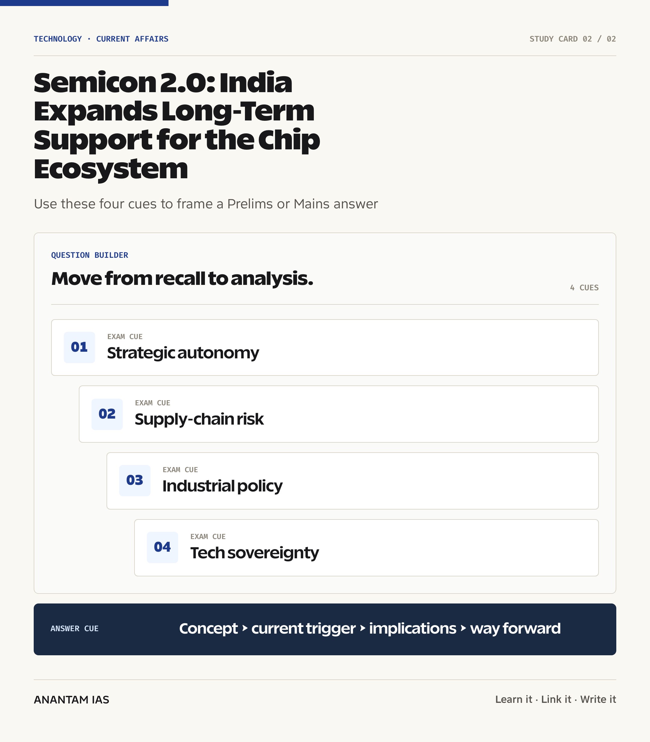
- Assess Semicon 2.0 as an industrial-policy intervention linking science and technology, manufacturing, infrastructure, start-ups and strategic autonomy.
- Examine how design IP, fabrication, packaging, materials and equipment together determine domestic value addition and supply-chain resilience.
- Analyze the case for public support in a sector marked by high capital cost, long gestation, rapid technological change and strong global concentration.
- Balance semiconductor expansion with reliable utilities, resource efficiency, skilled employment and transparent evaluation of public expenditure.
GS Paper 2
- Study the role of Centre-State coordination in land, power, water, logistics, skilling and investment facilitation for semiconductor clusters.
- Evaluate how international technology partnerships can support capability building without creating a new form of strategic dependence.
Essay
- Strategic autonomy in technology means building the capacity to choose and withstand shocks, not pursuing complete isolation from global networks.
Background and Context
How the semiconductor value chain works
A chip reaches an end user through several specialized stages, and weakness at any stage can limit the value captured within India.
- At the design stage, engineers translate product requirements into circuit architecture, logic, layouts and reusable intellectual-property cores. EDA tools help simulate and verify the design before an expensive manufacturing run.
- A wafer fab creates microscopic circuit patterns on silicon or another semiconductor substrate through repeated deposition, lithography, etching, implantation and cleaning steps. It is the capital-intensive front end of chip production.
- After fabrication, wafers are cut into dies. ATMP means Assembly, Testing, Marking and Packaging; OSAT describes outsourced providers that perform comparable back-end services for chip companies.
- Packaging isn’t a cosmetic shell. Advanced packaging connects dies, manages heat and power, protects devices and can integrate multiple chiplets or functions into one system-level package.
- The ecosystem also depends on ultra-pure materials, specialty gases, chemicals, precision equipment, clean rooms and reliable logistics. Localizing these inputs can reduce disruption risk and create opportunities beyond a few large fabs.
- The nanometre node is a technology-generation label. Mature nodes such as those in the 28-110 nm range remain relevant for many automobiles, industrial controls, power devices, connectivity products and consumer applications.
Institutional foundation under Semicon 1.0
Semicon 2.0 extends a mission architecture created after pandemic-era shortages exposed the concentration of global chip supply.
- The Union Cabinet approved the original Semicon India Programme in December 2021 with an outlay of ₹76,000 crore for semiconductor and display manufacturing and design.
- The India Semiconductor Mission was established as the nodal agency for strategy and implementation. Official material places it within Digital India Corporation with administrative and financial autonomy.
- The policy basket covered silicon and display fabs, compound semiconductors and sensors, ATMP/OSAT facilities, and the Design Linked Incentive route for domestic chip design.
- Existing modified schemes have offered eligible fabs fiscal support linked to 50% of project cost. The exact allocation and operating guidelines for the expanded Semicon 2.0 outlay must be read from its notified rules, not assumed from the earlier scheme.
- This institutional frame connects with India’s emerging technology ecosystem, where semiconductor capability supports digital infrastructure, artificial intelligence, telecom, space and advanced manufacturing.
The six pillars of Semicon 2.0
The Cabinet has framed the next phase as a full-ecosystem programme rather than a fab-only subsidy package.
- Design: support will deepen indigenous chip and system design, reusable intellectual property and strategic as well as commercial products, building on start-ups already using industry-standard design infrastructure.
- Machines and materials: incentives will reach firms producing or researching semiconductor equipment, materials, chemicals and gases, with spillovers expected for India’s precision-manufacturing base.
- More fabs: India will seek silicon, compound-semiconductor, discrete-component and display fabs. The first fab under the existing pipeline is scheduled to be commissioned in 2028.
- Advanced packaging: the programme will further strengthen ATMP/OSAT and attract more sophisticated technologies, an important step because packaging increasingly shapes chip performance, cost and system integration.
- Research and development: work that began around the 28-110 nm range will be extended toward more advanced nodes and technologies through collaboration with leading research centres in India and abroad.
- Talent development: training will move beyond chip design into clean-room operations, fab construction and other production skills, with industry involvement intended to make college training more job-relevant.
What the first phase has delivered
The Cabinet’s case for long-term support rests on an initial pipeline that now spans fabrication, packaging and design.
- PIB recorded 12 approved manufacturing units with cumulative proposed investment of more than ₹1.64 lakh crore under the earlier phase.
- The mix comprises one silicon fab, one silicon-carbide fab, an integrated gallium-nitride Micro LED display fab and nine packaging units serving multiple downstream sectors.
- Three facilities associated with Micron, Kaynes and CG Semi had begun commercial production when the Cabinet release was issued. This marks movement from approvals and construction toward operating output.
- On design, 24 projects from start-ups and MSMEs had been approved for financial support, while 105 start-ups or MSMEs had access to industry-standard EDA tools.
- Supported design applications include satellite communications, drones, surveillance, Internet of Things devices, LED drivers, AI systems, telecom equipment and smart meters, showing demand across civilian and strategic markets.
- PIB also reported 315 universities using current EDA tools for complex chip-design training and about 68,000 students trained, creating a base that Semicon 2.0 intends to deepen.
Why a complete ecosystem matters
A domestic fab can still remain highly exposed if its tools, inputs, intellectual property, maintenance and customers depend on concentrated foreign sources.
- Supply-chain resilience comes from alternative suppliers, inventories, trusted logistics and some domestic capability across critical stages; it doesn’t require every input to be produced entirely within one country.
- Strategic autonomy improves when India can design priority chips, assure selected production and packaging capacity, and recover faster from geopolitical restrictions, disasters or transport disruptions.
- Domestic design IP can raise value capture because reusable cores, architectures and system knowledge often shape product differentiation even when manufacturing is contracted to a foundry.
- Equipment, chemicals and packaging widen the supplier base for MSMEs and precision manufacturers. They also create capabilities that can serve electronics, medical devices, energy systems and advanced industrial production.
- The goal should be trusted interdependence: deeper domestic capacity combined with diversified partnerships for technology, equipment, research, finance and access to global markets.
Key implementation risks
Large public outlays can create durable capability only when project selection, infrastructure and accountability move together.
- Semiconductor projects have high capital costs and long gestation. Delays in construction, tool installation, customer qualification or demand can weaken commercial viability even after an approval is announced.
- Fabs need dependable high-quality power, water, waste treatment, logistics and clean-room services. State incentives can’t compensate for unreliable industrial infrastructure over the full operating life of a plant.
- Rapid technology cycles create an obsolescence risk. Policy appraisal should test the target market, process maturity, upgrade path and committed customers instead of treating a smaller node as automatically superior.
- Access to leading tools, equipment and know-how remains globally distributed. India must manage export controls, licensing restrictions and supplier concentration through diversification and credible international partnerships.
- Public support needs milestone-based disbursement, disclosure and independent evaluation. Metrics should track commissioned capacity, yields, domestic value addition, patents, skilled jobs and commercial sales, not approvals alone.
Way Forward
Sequence support around credible markets
- Prioritize projects with clear technology partners, customer commitments, financing and upgrade plans; match the type of fab or packaging capacity to realistic domestic and export demand.
- Use milestone-based incentives tied to construction, tool installation, qualification, production, yield improvement and sales rather than treating approval as the final outcome.
Build shared industrial public goods
- Develop cluster-level power, water recycling, effluent treatment, logistics, testing and emergency services that lower operating risk for anchor firms and smaller suppliers.
- Expand shared access to EDA tools, multi-project wafer runs, prototyping, metrology and certification so start-ups and universities can cross the gap between a design and a manufacturable product.
Connect design, manufacturing and skills
- Create procurement and commercialization pathways for Indian-designed chips in suitable telecom, mobility, energy, space and public-infrastructure applications, subject to rigorous quality and security testing.
- Build apprenticeship routes with operating plants and equipment firms for process, maintenance, packaging and clean-room skills, while keeping advanced research linked to universities and national laboratories.
Protect resilience and public value
- Diversify global partnerships for tools, materials, technology and research; avoid replacing dependence on one concentrated supplier network with dependence on another.
- Publish a periodic outcome dashboard covering projects commissioned, production, yields, domestic sourcing, patents, commercialized designs, skilled jobs, resource use and public support disbursed.
Conclusion
Semicon 2.0 recognizes that chip capability is an ecosystem outcome. Design talent alone can’t assure supply, and a fab alone can’t create autonomy without materials, equipment, packaging, research, customers and skilled operations around it.
The ₹1,27,500 crore commitment can strengthen India’s technological choices if it converts public support into operating capacity, indigenous knowledge and competitive suppliers. The decisive measures will be commissioning, reliable production, domestic value addition and resilience, not the number of announcements.
UPSC Practice Questions
Prelims MCQ 1
With reference to Semicon 2.0, consider the following statements:
- Its six pillars include chip design, machines and materials, fabrication, advanced packaging, research and development, and talent development.
- ATMP and OSAT refer primarily to front-end circuit fabrication on semiconductor wafers.
- The Cabinet release states that the first fab in the existing programme pipeline is scheduled for commissioning in 2028.
How many of the above statements are correct?
(a) Only one (b) Only two (c) All three (d) None
Answer: (b) Only two
Explanation:
Statements 1 and 3 are correct. ATMP/OSAT are back-end assembly, testing, marking and packaging functions; wafer fabrication is the front-end process, so statement 2 is incorrect.
Prelims MCQ 2
Which one of the following best distinguishes a semiconductor fab from an OSAT facility?
(a) A fab designs only software, while an OSAT produces silicon wafers (b) A fab fabricates circuits on wafers, while an OSAT assembles, tests and packages dies (c) A fab manufactures display glass only, while an OSAT produces specialty gases (d) A fab regulates chip imports, while an OSAT licenses design intellectual property
Answer: (b) A fab fabricates circuits on wafers, while an OSAT assembles, tests and packages dies
Explanation:
A fab performs front-end wafer processing. An OSAT is an outsourced provider of back-end assembly and test services, often including packaging and final qualification.
UPSC Mains Questions
- Semicon 2.0 marks a shift from attracting individual plants to building a complete semiconductor ecosystem. Discuss how its six-pillar approach can improve domestic value addition and supply-chain resilience. What implementation conditions will determine whether the public outlay creates durable capability?
- Semiconductor fabrication involves high capital cost, long gestation and rapid technological change. Examine the case for mission-oriented industrial policy in this sector. Suggest safeguards that can reconcile strategic objectives with fiscal accountability, commercial viability and environmental responsibility.
- Technological self-reliance doesn’t mean isolation from global value chains. In the context of India Semiconductor Mission, evaluate how India can combine indigenous design, manufacturing and skills with diversified international partnerships while limiting new forms of strategic dependence.
Sources: PIB, Cabinet and PIB, Ministry of Electronics and Information Technology.
Frequently Asked Questions
What is Semicon 2.0?
Semicon 2.0 is the next phase of India’s semiconductor policy, approved by the Union Cabinet on 15 July 2026 with a ₹1,27,500 crore outlay. It seeks to build a complete ecosystem covering design, equipment and materials, fabrication, advanced packaging, research and talent rather than support manufacturing plants in isolation.
What are its six pillars?
The six pillars are chip design; semiconductor machines and materials; more silicon, compound, discrete and display fabs; stronger ATMP/OSAT and advanced packaging; research and development for advanced technologies; and talent development spanning design, clean rooms, fab construction and production-oriented skills.
How does it differ from Semicon 1.0?
Semicon 1.0 created the institutional and incentive base and produced an initial pipeline of fabs, packaging units and design projects. Semicon 2.0 builds on that base with a larger long-term commitment and sharper emphasis on the full value chain, especially equipment, materials, advanced packaging, R&D and deeper workforce capability.
What do ATMP and OSAT mean?
ATMP stands for Assembly, Testing, Marking and Packaging. OSAT means Outsourced Semiconductor Assembly and Test, referring to specialist firms that provide back-end services for chip companies. These stages turn fabricated dies into protected, connected and tested products that can be installed in electronic systems.
Why are mature process nodes still useful?
A mature process node can offer proven reliability, adequate performance and lower development risk for many products. Automobiles, industrial controls, power management, connectivity devices and consumer electronics don’t always need the smallest node. Policy should match node choice to application, customers, cost and a credible upgrade path.
Why does semiconductor resilience matter?
Chips support critical infrastructure, defence, telecom, transport, energy and digital services. A disruption in fabrication, materials, equipment or packaging can spread across many industries. Resilience means building selected domestic capabilities, diversifying trusted suppliers and partnerships, and preserving the ability to maintain essential systems during external shocks.
Tell Google you want more of this.
Add Anantam IAS as a preferred sourceOne tap, and this site shows up more often in your own Top Stories, AI Overviews and AI Mode. Remove it any time.