

Why in News?
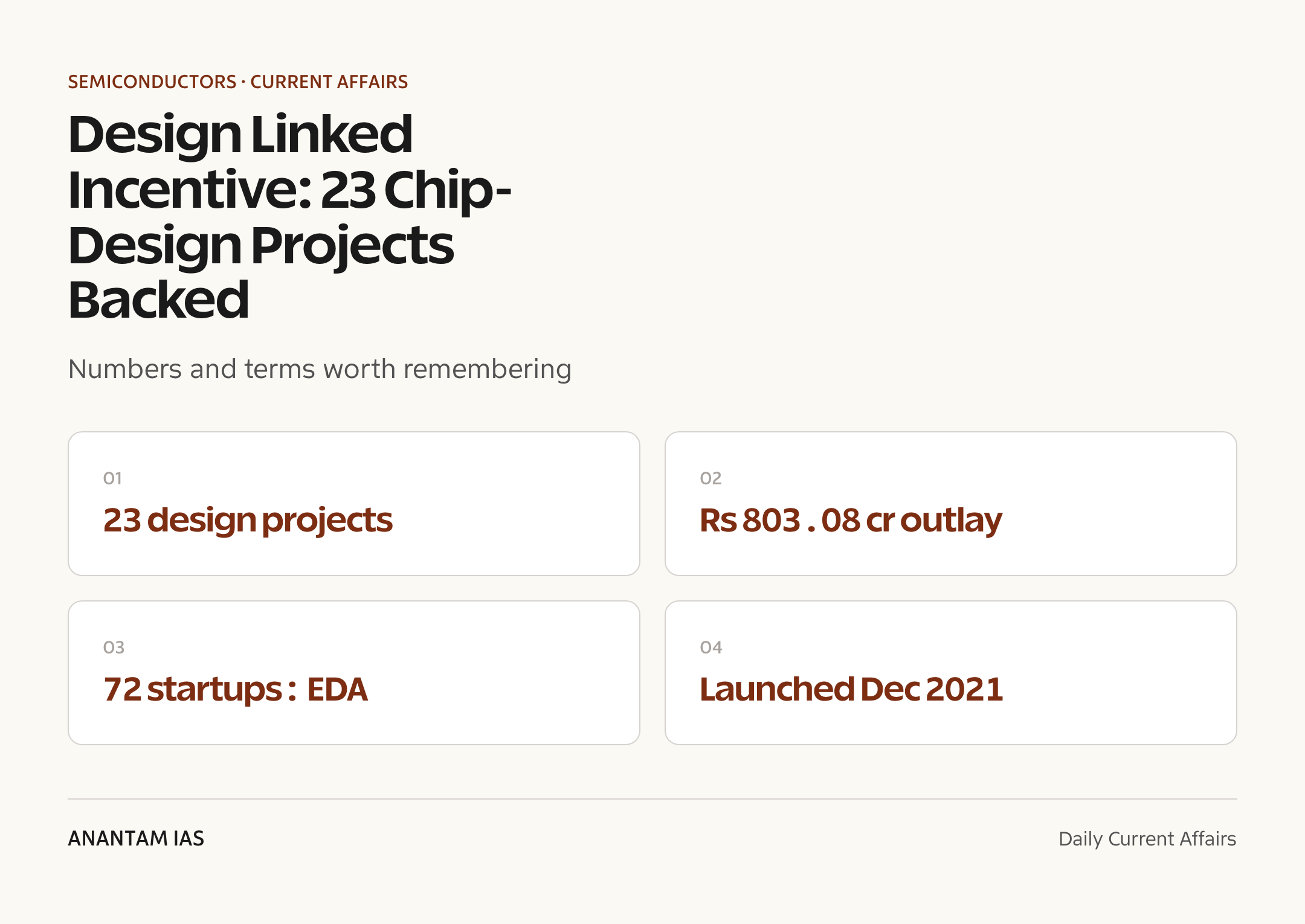
The Ministry of Electronics and IT (MeitY) told the Lok Sabha on 30 July 2025 that 23 chip-design projects from domestic firms, startups and MSMEs have been sanctioned financial support under the Design Linked Incentive (DLI) Scheme, the design-led pillar of the India Semiconductor Mission.
A total project outlay of Rs 803.08 crore, including the cost of Electronic Design Automation (EDA) tools, has been approved under the scheme, with funds released against defined milestones up to chip deployment.
- 23 firms and startups sanctioned support to design chips for surveillance cameras, energy meters, microprocessor IP cores and networking applications.
- Approved outlay so far: Rs 803.08 crore, inclusive of EDA-tool costs.
- 72 startups (under DLI) and 278 academic institutions (under the Chips-to-Startup, or C2S, programme) have been approved for access to advanced EDA tools.
- 10 companies have raised venture-capital funding to scale prototypes; 6 have completed prototype tape-outs at foundries.
- 20 chip designs from 17 academic institutions fabricated by SCL, Mohali (the Semi-Conductor Laboratory).
- Disclosed by Minister of State Jitin Prasada in a written Lok Sabha reply.
The development matters in the context of:
- Design — not just fabrication — is where most of a chip’s value is captured, so a design-led base reduces dependence on foreign IP.
- DLI targets the core market-failure in chip design: high entry barriers, long development timelines and the cost of licensed EDA tools and IP cores.
- Builds a homegrown talent and startup pipeline that can feed the upcoming fabs under the wider Semicon India Programme.

UPSC Relevance
Prelims Relevance
- DLI Scheme — launched December 2021, outlay Rs 1,000 crore, implemented by MeitY.
- Semicon India Programme total outlay Rs 76,000 crore; DLI is one component.
- DLI offers: design-infrastructure support (EDA tools, IP cores), a Product Design Linked Incentive and a Deployment Linked Incentive.
- Product incentive: up to 50% of eligible cost, capped at Rs 15 crore per application.
- Deployment incentive: 6% to 4% of net sales over five years, capped at Rs 30 crore per application.
- EDA = Electronic Design Automation; IP cores = reusable design blocks.
- C2S (Chips-to-Startup) programme builds chip-design skills in academia; 278 institutions covered.
- SCL, Mohali — Semi-Conductor Laboratory under the Department of Space, India’s lone operating fab line.
- ISM (India Semiconductor Mission) is the nodal agency steering semiconductor incentives.
- A tape-out is the final stage of design sent for fabrication.
Mains Relevance
GS Paper 3
- Semiconductors as a critical and strategic technology; design-led self-reliance and the chip value chain.
- Industrial-policy tools — production-linked vs design-linked incentives — and their fit for a deep-tech startup ecosystem.
GS Paper 2
- Government schemes for the electronics sector and the role of academia-industry-startup linkages in technology missions.
Essay
- Self-reliance in critical technologies: building from the design end up.
- From assembly to design: where a developing economy should place its industrial bets.
Background and Context
What the DLI Scheme is
The Design Linked Incentive Scheme funds the design end of the chip value chain.
- Approved with an outlay of Rs 1,000 crore and launched in December 2021 under MeitY.
- It is the design pillar of the broader Semicon India Programme (total outlay Rs 76,000 crore).
- Aim — support domestic companies, startups and MSMEs through the full cycle: design, prototyping, scaling and commercialisation.
- It tackles the structural barriers of chip design: high entry costs, long timelines and stiff global competition.
How the incentives are structured
DLI works through three layers of support rather than a single subsidy.
- Design infrastructure support — access to EDA tools and IP cores for early prototyping, lowering the steep cost of licensed software.
- Product Design Linked Incentive — up to 50% of eligible expenditure, capped at Rs 15 crore per application, for prototyping, scale-up and volume production.
- Deployment Linked Incentive — 6% to 4% of net sales turnover over five years, capped at Rs 30 crore per application, for actual deployment of chip solutions.
- Funds release is milestone-linked, including the deployment of finished chips.
The July 2025 numbers
As of the Lok Sabha reply, the scheme had built a measurable design portfolio.
- 23 firms and startups sanctioned support for chips serving surveillance cameras, energy meters, microprocessor IPs and networking.
- Approved project outlay of Rs 803.08 crore, including the cost of EDA tools.
- 72 startups and 278 academic institutions approved for state-of-the-art EDA-tool access.
- 10 firms raised VC funding; 6 completed prototype tape-outs at foundries.
- 20 chip designs from 17 institutions fabricated by SCL, Mohali.
Where it sits in the India Semiconductor Mission
DLI is one of several incentive tracks under the Semicon India Programme.
- Modified Semiconductor Fab Scheme — incentives for setting up silicon-based fabrication units.
- Compound Semiconductor / ATMP / OSAT Scheme — for assembly, testing, marking and packaging units.
- SPECS (Scheme for Promotion of Manufacturing of Electronic Components and Semiconductors) supports component-level manufacturing.
- DLI covers the design end; the ISM acts as the nodal agency coordinating the programme.
- Together they aim to cover the chain from design to fabrication to packaging.
Why design-led matters
A design base gives India strategic leverage that fabs alone do not.
- Chip design and IP capture a large share of the value and are far less capital-intensive than a fab.
- India already supplies a big slice of the world’s chip-design engineering talent; DLI tries to convert that into India-owned products and IP.
- Domestic IP in surveillance, metering and networking chips has direct national-security and critical-infrastructure relevance.
- A design-startup pipeline can later feed the fabs being set up under the manufacturing schemes.
Constraints and concerns
The scheme’s scale and uptake remain modest against the ambition.
- The Rs 1,000 crore DLI outlay is small beside the Rs 76,000 crore manufacturing-heavy programme.
- Only 23 design firms sanctioned so far — a thin base for a globally competitive ecosystem.
- Dependence on foreign-owned EDA tools and IP cores persists despite subsidised access.
- Long timelines mean tape-outs and commercial revenue trail the sanctioning by years.
Way Forward
Deepen the design base
- Scale beyond the first 23 firms with a larger DLI corpus and faster, milestone-light disbursal for early-stage startups.
- Strengthen the C2S academic pipeline so institutional designs convert into spin-off startups.
Reduce tool dependence
- Back development of indigenous EDA tools and open IP libraries to cut recurring licence costs.
- Expand fabrication access at SCL, Mohali and upcoming fabs so designs can be taped out domestically.
Link design to demand
- Use government procurement in surveillance, smart metering and telecom to create assured demand for India-designed chips.
- Pair DLI with patient capital and design-services anchors to bridge the prototype-to-product gap.
Conclusion
The DLI Scheme’s July 2025 scorecard — 23 sanctioned design projects, a Rs 803 crore outlay and EDA access for 72 startups and 278 institutions — shows India trying to build semiconductor self-reliance from the design end, not just chase fabs.
The numbers are encouraging but early. Converting subsidised design access into commercially deployed, India-owned chips, and reducing dependence on foreign tools and IP, will decide whether the design-led pillar of the India Semiconductor Mission delivers strategic depth.
UPSC Practice Questions
Prelims MCQ 1
With reference to the Design Linked Incentive (DLI) Scheme, consider the following statements:
- It is implemented by the Ministry of Electronics and Information Technology.
- It supports the fabrication of silicon wafers through dedicated foundry subsidies.
- It provides design-infrastructure support such as EDA tools and IP cores.
How many of the above statements are correct?
(a) Only one (b) Only two (c) All three (d) None
Answer: (b) Only two
Explanation:
Statements 1 and 3 are correct. DLI is a MeitY scheme offering EDA tools, IP cores and design incentives. It targets chip design, not wafer fabrication — fab subsidies fall under the separate Modified Fab Scheme; so statement 2 is wrong.
Prelims MCQ 2
Under the DLI Scheme, the Product Design Linked Incentive provides financial support of:
(a) Up to 50% of eligible cost, capped at Rs 15 crore per application (b) Up to 25% of eligible cost, capped at Rs 30 crore per application (c) A flat Rs 100 crore per firm (d) 6% to 4% of net sales over five years
Answer: (a) Up to 50% of eligible cost, capped at Rs 15 crore per application
Explanation:
The product incentive covers up to 50% of eligible cost, capped at Rs 15 crore per application. The 6%-4% of net sales (option d) is the separate Deployment Linked Incentive, capped at Rs 30 crore.
UPSC Mains Questions
- Design-led self-reliance is being positioned as a core pillar of the India Semiconductor Mission. Examine the rationale for incentivising chip design alongside fabrication, and assess the early outcomes of the Design Linked Incentive Scheme.
- Industrial policy for critical technologies must address market failures, not just offer subsidies. In this light, evaluate how India’s mix of design-linked and production-linked incentives seeks to build a domestic semiconductor ecosystem.
Sources: PIB, Ministry of Electronics and IT and Ministry of Electronics and IT (MeitY).
Frequently Asked Questions
What is the Design Linked Incentive Scheme?
The DLI Scheme is a MeitY programme launched in December 2021 with a Rs 1,000 crore outlay. It supports Indian companies, startups and MSMEs across semiconductor design and commercialisation by providing EDA tools, IP cores and financial incentives for prototyping, scaling and deployment of chips.
How many projects have been sanctioned under DLI?
As of the July 2025 Lok Sabha reply, 23 firms and startups had been sanctioned financial support to design chips for surveillance cameras, energy meters, microprocessor IPs and networking. A total project outlay of Rs 803.08 crore, including EDA-tool costs, has been approved under the scheme.
How does DLI fit into the India Semiconductor Mission?
DLI is the design-led pillar of the Semicon India Programme, which has a total outlay of Rs 76,000 crore. While fab, ATMP/OSAT and SPECS schemes cover manufacturing and components, DLI funds chip design, with the India Semiconductor Mission acting as the nodal coordinating agency.
What incentives does the DLI Scheme offer?
DLI offers three layers: design-infrastructure support (EDA tools and IP cores); a Product Design Linked Incentive of up to 50% of eligible cost capped at Rs 15 crore per application; and a Deployment Linked Incentive of 6% to 4% of net sales over five years, capped at Rs 30 crore per application.
What are EDA tools and why do they matter?
EDA, or Electronic Design Automation, is the licensed software used to design and verify integrated circuits. It is expensive and a major entry barrier. By subsidising access for 72 startups and 278 academic institutions, DLI lowers the cost of entering chip design.
What role does SCL, Mohali play?
The Semi-Conductor Laboratory at Mohali is India’s main operating fabrication line, under the Department of Space. By July 2025 it had fabricated 20 chip designs from 17 academic institutions, letting Indian designers tape out and test chips domestically rather than abroad.
Tell Google you want more of this.
Add Anantam IAS as a preferred sourceOne tap, and this site shows up more often in your own Top Stories, AI Overviews and AI Mode. Remove it any time.