

Solar electricity is already cheaper than coal in most of India. The question that’s defined the last few years isn’t whether solar wins on cost, it’s how much further the cost can fall, and how high the efficiency ceiling really is for photovoltaic technology. Perovskite Solar Cells are the answer most of the research community is converging on. They’ve gone from a curious lab finding in 2009 to laboratory efficiencies above 26% by 2024-25, and tandem perovskite-silicon cells are now crossing 33% in certified measurements. That’s a frontier almost nobody saw coming a decade ago.
The Perovskite Solar Cells story is a textbook case of what happens when materials science, manufacturing economics, and policy alignment all push in the same direction. India has every reason to care. The country has committed to 500 GW of non-fossil capacity by 2030 under its updated NDC and energy transition framework, and solar is the single largest pillar in that plan. If perovskite technology delivers what the lab numbers suggest, the cost-per-watt of utility-scale solar could drop another 30-50% by the end of the decade. That changes what “energy transition” actually looks like in a country still adding new coal even as it adds record solar.
This piece works through what perovskite is, why it’s a step-change rather than an incremental improvement, where the engineering challenges remain, and what India’s research and industrial response should look like.
Quick Facts at a Glance
- What they are: Solar cells using a perovskite-structured material (typically methylammonium lead halide or formamidinium-cesium lead halide) as the light-absorbing layer
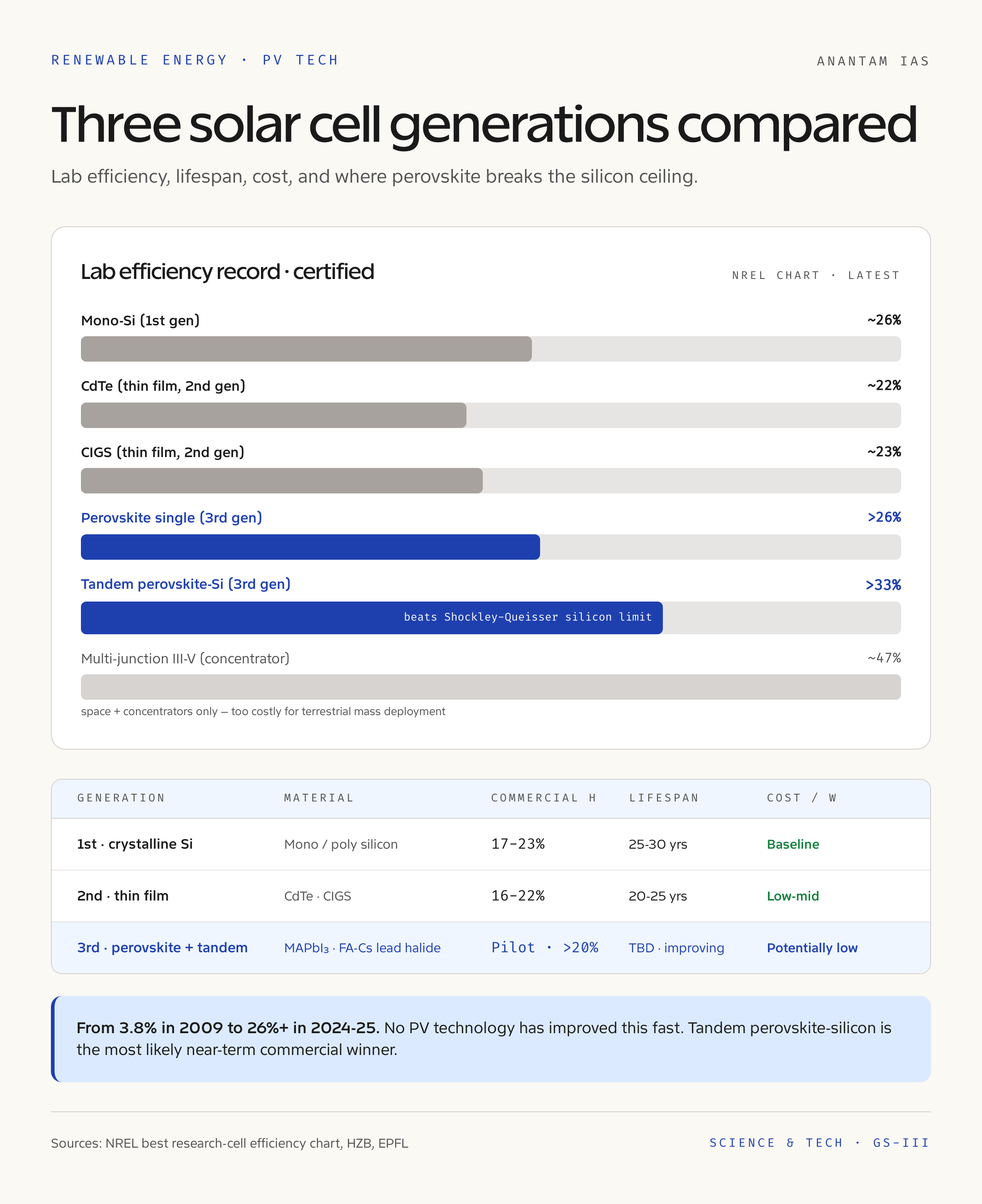
- Lab efficiency record (single-junction): Above 26% (2024-25 certified)
- Tandem perovskite-silicon record: Above 33% (2024-25 certified)
- Theoretical limit (Shockley-Queisser, single junction): ~33%; tandems can exceed 40%
- Cost advantage: Solution-based fabrication at low temperatures, low capex per GW
- Key Indian players: IIT Bombay, IIT Madras, IISc Bengaluru, NCL Pune, ISRO, NIT Trichy, several Indian startups
- Policy frame: National Solar Mission, PLI for solar PV, BIS standards, CEA grid code
Why in News: Tandem Cells Cross a Commercial Threshold
In late April and early May 2026, multiple research groups including teams at HZB Berlin, KAUST, EPFL, and Indian institutions reported continued progress in stabilizing perovskite-silicon tandem cells at high efficiency, with several major manufacturers (Oxford PV, Trinasolar, JinkoSolar, LONGi) signaling commercial deployment timelines. This wave of progress comes alongside India’s accelerating solar deployment, with cumulative installed solar capacity crossing milestones through 2025-26 and the Production Linked Incentive (PLI) scheme expanding domestic module manufacturing.
For Indian policy, this matters because the next 5-7 years will see a generational technology transition in solar manufacturing. India’s PLI bets are still primarily silicon-centric. A clear-eyed assessment of when and how to add perovskite or tandem capacity into the domestic mix will determine whether India is buying perovskite modules in 2030 or making them.
Background and Historical Context
Solar cells fall into rough generations. First-generation cells are crystalline silicon, both monocrystalline and polycrystalline. They’ve dominated the market for over four decades, with current commercial efficiencies of 20-23% and theoretical limits around 29% under single-junction conditions. Second-generation thin-film cells, including cadmium telluride (CdTe) and copper indium gallium selenide (CIGS), occupy a smaller niche, particularly in utility-scale installations.
Third-generation cells include organic photovoltaics, dye-sensitized cells, quantum dot cells, and perovskites. Perovskite cells are named for their crystal structure (ABX3, the same general structure as the calcium titanate mineral perovskite). The light-absorbing layer is typically a hybrid organic-inorganic compound like methylammonium lead iodide (MAPbI3), or more recently, mixed-cation mixed-halide formulations using formamidinium and cesium for improved stability.
The first perovskite solar cell was reported in 2009 with about 3.8% efficiency. Within a decade, it crossed 25%. That kind of efficiency improvement curve, faster than any other PV technology in history, is what put perovskite on every clean energy roadmap.
The reason perovskites improved so fast is partly chemistry, partly fabrication economics. Perovskite films can be deposited from solution at relatively low temperatures (often under 150 degrees Celsius), unlike silicon which requires high-temperature processing in vacuum. That means lower capex per gigawatt of manufacturing, faster scale-up, and the possibility of roll-to-roll printing on flexible substrates. Combine that with high tunable bandgap and you get a technology ideally suited for tandem cells, where a perovskite top cell absorbs blue and green light while a silicon bottom cell absorbs red and infrared, raising overall efficiency well above what either can achieve alone.
Our coverage of thermal electricity and energy poverty in India provides the broader energy mix context this perovskite story sits inside.
How It Works: From Photon to Electron
A solar cell’s job is conceptually simple. Convert photons (light) into electrons (current) through a semiconductor that creates an internal electric field separating positive and negative charges.
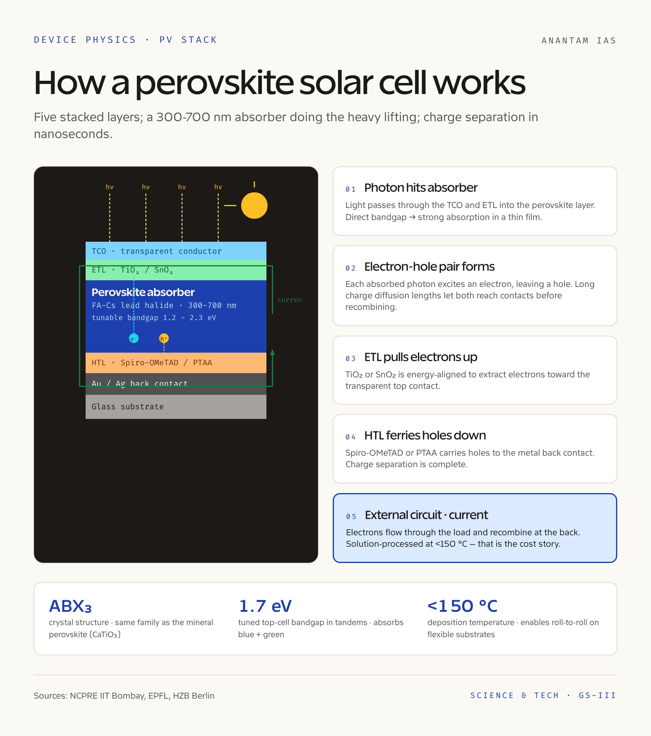
In a perovskite solar cell, light hits the perovskite absorber layer (typically 300-700 nanometers thick). Each absorbed photon generates an electron-hole pair. The cell architecture sandwiches the perovskite between two charge-transport layers: an electron transport layer (often TiO2 or SnO2) on one side and a hole transport layer (often Spiro-OMeTAD or PTAA) on the other. These layers extract electrons and holes to opposite sides of the device. Transparent conducting oxide (TCO) on the top, metal contact on the bottom, and you have a working cell.
What makes perovskite remarkable:
- Direct bandgap. Strong light absorption in a thin film, unlike silicon which is an indirect bandgap material requiring thicker layers.
- Tunable bandgap. By changing halide composition (iodide, bromide, chloride mix), the bandgap can be tuned from about 1.2 eV to 2.3 eV, useful for tandem applications.
- Long charge diffusion lengths. Despite being made from imperfect crystals, perovskites let charges travel hundreds of nanometers without recombining, enough to be collected.
- Defect tolerance. Perovskite materials remain efficient even with significant point defects, a property that’s still actively researched.
In a tandem perovskite-silicon cell, the perovskite top layer is bandgap-tuned to about 1.7 eV, absorbing blue and green light. Light not absorbed passes through to the silicon below (1.1 eV bandgap), which absorbs red and infrared. The two cells are connected electrically (in two-terminal monolithic tandems, through a recombination junction). Total efficiency exceeds either cell alone, with current certified records above 33%.
Why It Matters: Five Reasons This Reshapes Solar Economics
One, lower cost per watt. Solution-processed perovskite manufacturing has lower capex per GW than silicon. Combine that with higher efficiency, and the cost-per-watt of installed solar drops materially.
Two, less land per gigawatt. Higher-efficiency modules mean fewer modules per gigawatt, less land, less mounting infrastructure, less cabling. For India, where solar farms compete with agriculture for land, this matters.
Three, flexibility opens new markets. Roll-to-roll perovskite on flexible substrates can be integrated into roofs that can’t take rigid panels, into vehicle surfaces, into building facades, into agricultural structures.
Four, less energy payback time. The energy required to make a perovskite cell is lower than for silicon, which means the cell pays back its embodied energy faster. Important for genuinely low-carbon manufacturing.
Five, new manufacturing models. Perovskite production is more compatible with smaller, distributed manufacturing than gigafab-style silicon. That changes who can play in solar manufacturing globally and within India.
Detailed Analysis
India’s Perovskite Research Ecosystem
Indian institutions have a strong perovskite research base. IIT Bombay’s National Centre for Photovoltaic Research and Education runs sustained programs on perovskite stability, encapsulation, and module-scale fabrication. IIT Madras has pushed on charge transport layer engineering. IISc Bengaluru has world-class perovskite materials chemistry groups. NCL Pune and CSIR labs are working on scalable synthesis. ISRO’s research wings have looked at perovskite for space applications, where weight-per-watt is critical.
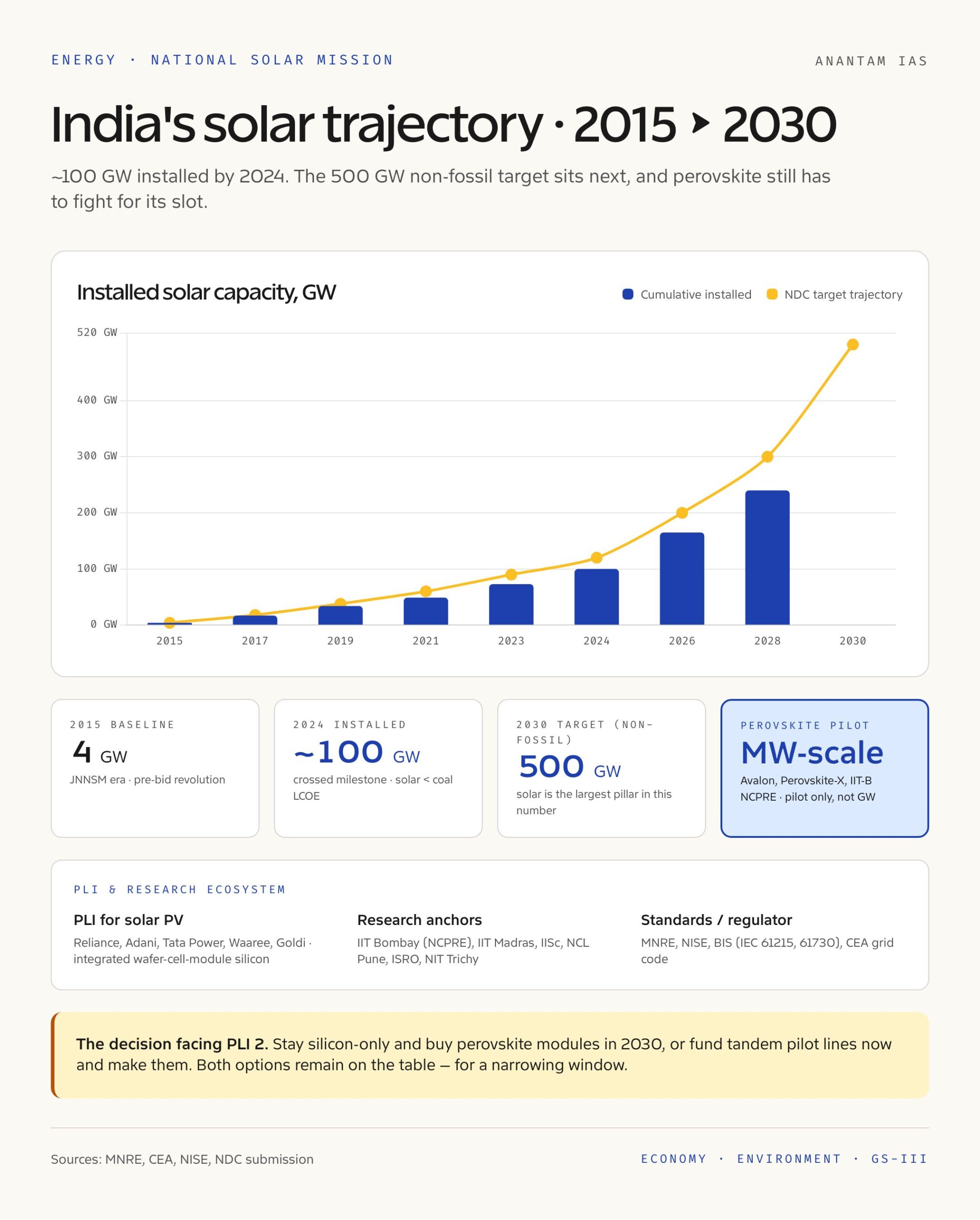
What’s been thinner is industry-academia translation. Indian solar manufacturing remains overwhelmingly silicon. A few Indian startups (Avalon Solar, Perovskite-X, others) are working on perovskite, but at pilot rather than gigawatt scale. The gap between lab cell records and commercial-scale modules, especially when accounting for stability, is large and well-known. Closing it needs sustained funding, dedicated translational facilities, and clear policy signals.
National Solar Mission and PLI
The Jawaharlal Nehru National Solar Mission was launched in 2010 with an initial target of 20 GW by 2022, later revised upward dramatically. India crossed 100 GW of installed solar capacity around 2024 and is on a trajectory toward 500 GW non-fossil by 2030. Domestic manufacturing has been pushed through the PLI scheme, with major outlays for solar PV manufacturing. Companies like Reliance, Adani, Tata Power, Waaree, and Goldi Solar are scaling integrated wafer-cell-module manufacturing.
Most of this build-out is silicon-based. The PLI scheme’s tranches are technology-agnostic in principle but heavily silicon in practice. Adding a perovskite or tandem-specific component, with funded pilot lines and reliability testing infrastructure, would position India for the next technology wave rather than reacting to it.
For broader green-economy context, our explainer on globalization and Indian economy frames why technology choices in solar matter for India’s industrial trajectory.
Stability: The Make-or-Break Question
The biggest open question for perovskite is stability. Lab cells degrade under heat, moisture, oxygen, and UV exposure. Commercial silicon panels carry 25-30 year warranties. Perovskite needs to match or come close to that for utility-scale deployment to make sense.
The community has made significant progress. Encapsulation strategies, mixed-cation chemistries, ion migration suppression, interface engineering, and accelerated lifetime testing protocols have all advanced. But the gap between best lab stability (a few thousand hours under standard test conditions) and 25-year field warranty is still meaningful. Tandem perovskite-silicon cells inherit silicon’s known reliability for the bottom cell, which is one reason they’re moving faster toward commercial deployment than single-junction perovskite.
Comparative Perspective
| Technology | Commercial Efficiency | Lab Record | Lifespan | Cost/W |
|---|---|---|---|---|
| Mono-Si | 20-23% | ~26% | 25-30 years | Baseline |
| Poly-Si | 17-20% | ~24% | 25-30 years | Baseline-low |
| CdTe (thin film) | 19-22% | ~22% | 25 years | Low |
| CIGS | 16-20% | ~23% | 20-25 years | Mid |
| Perovskite (single) | Pilot | >26% | TBD (improving) | Potentially low |
| Tandem Perovskite-Si | Pilot | >33% | TBD | Premium initially |
| Multi-junction (III-V) | 30%+ | 47% (under concentration) | Long | Very high |
Tandem perovskite-silicon is the most likely near-term commercial winner. Multi-junction III-V cells are amazing but stay confined to space and concentrator applications because they’re too expensive for terrestrial mass deployment. Perovskite single-junction cells will find niches in flexible and BIPV (building-integrated photovoltaic) applications even before they fully solve stability.
Challenges and Critiques
The perovskite story is real, the obstacles are also real.
Lead toxicity. Most high-efficiency perovskites use lead. Lead leaching during module damage or end-of-life is an environmental concern. Tin and other lead-free alternatives exist but lag in efficiency.
Stability under field conditions. Lab tests don’t capture monsoon humidity, dust, temperature swings, and UV in real Indian deployment. More field validation is needed.
Manufacturing scale-up. Going from a 1 cm-squared cell at 26% to a 1 m-squared module at 22% with high yield is a different problem. Many materials look great in cells and underperform in modules.
Recycling and end-of-life. Perovskite modules will eventually need recycling pathways, especially given lead content. India needs an EPR (extended producer responsibility) framework for solar that anticipates this.
Standards and certification. International testing standards (IEC 61215, 61730) were designed around silicon. Perovskite-specific stability testing protocols are being developed. India’s BIS standards need to keep pace.
Industrial commitment. Indian solar manufacturers are scaling silicon under PLI. Asking them to add perovskite capacity now risks splitting investment. A separate, focused perovskite manufacturing track may be needed.
UPSC Prelims Pointers
- Perovskite materials have the ABX3 crystal structure, named after the mineral calcium titanate
- Methylammonium lead iodide (MAPbI3) was the first widely studied perovskite for solar cells
- The first perovskite solar cell was reported in 2009 with ~3.8% efficiency
- Tandem perovskite-silicon cells exceed 33% efficiency in lab certified measurements
- The Shockley-Queisser limit for single-junction silicon is approximately 29%
- The Jawaharlal Nehru National Solar Mission was launched in 2010 under the National Action Plan on Climate Change
- India has crossed 100 GW of installed solar capacity (around 2024)
- India targets 500 GW of non-fossil installed capacity by 2030
- The PLI scheme for solar PV manufacturing is administered by the Ministry of New and Renewable Energy (MNRE)
- The National Institute of Solar Energy (NISE) is the apex R&D institution under MNRE
Mains Practice Questions
- GS Paper III: Discuss the technological advantages of Perovskite Solar Cells over conventional silicon solar cells. How can India leverage this technology to meet its clean energy targets? (250 words)
- GS Paper III: “India’s solar manufacturing strategy must look beyond silicon.” Examine the case for incorporating perovskite and tandem solar cell technology into the PLI framework. (250 words)
- GS Paper III: Analyze the role of indigenous research institutions like IITs, IISc, and ISRO in advancing photovoltaic technology in India. What policy support is needed to translate research to commercial production? (150 words)
- GS Paper III: Discuss the environmental and lifecycle considerations of large-scale solar deployment in India, with reference to perovskite cells, lead toxicity, and end-of-life recycling. (250 words)
Way Forward
India’s solar transition is the largest infrastructure story of this decade. Getting the technology mix right matters far beyond the levelized cost calculations on any single project. The country needs three things from a perovskite strategy.
First, a dedicated funding line within the PLI architecture or a successor scheme for perovskite and tandem manufacturing pilot lines, with clear milestones tied to module-level efficiency, stability, and cost. Second, a sustained research push connecting IITs, IISc, NCL, ISRO, and industry through translational consortia, focused on stability, scale-up, and end-of-life recycling. Third, a regulatory framework that anticipates perovskite-specific issues, lead handling, BIS standards updates, EPR for solar waste, before they become field problems.
Perovskite Solar Cells aren’t a science fiction promise. They’re a near-term commercial technology that will be deployed in gigawatt scale globally within five years. India can either be a primary participant in that wave or a late buyer. The decisions that determine which it is are being made right now, in policy meetings and industry boardrooms that most people never see.
Frequently Asked Questions
What are perovskite solar cells?
Perovskite Solar Cells are photovoltaic devices using a perovskite-structured material (typically a hybrid organic-inorganic lead halide compound) as the light-absorbing layer. They achieve high efficiency through low-temperature, solution-based fabrication.
How efficient are perovskite solar cells?
Single-junction perovskite cells have crossed 26% efficiency in certified lab measurements. Tandem perovskite-silicon cells have crossed 33%, beating the practical efficiency limit of silicon alone.
Why are perovskite cells cheaper to make?
Perovskite films are deposited from solution at relatively low temperatures, unlike silicon which requires high-temperature vacuum processing. This means lower capital expenditure per gigawatt of manufacturing capacity.
What is a tandem solar cell?
A tandem cell stacks two photovoltaic materials with different bandgaps. The top cell absorbs higher-energy photons (like blue and green light) while the bottom cell absorbs lower-energy photons (red and infrared), achieving higher total efficiency.
What are the main challenges for perovskite solar cells?
The biggest challenges are long-term stability under field conditions, lead toxicity, scale-up from cells to modules with high yield, and developing recycling pathways for end-of-life modules.
How is India researching perovskite technology?
Indian institutions including IIT Bombay, IIT Madras, IISc Bengaluru, NCL Pune, and ISRO have active perovskite research programs. Pilot manufacturing exists but commercial gigawatt-scale perovskite production is not yet established in India.
Will perovskite replace silicon solar panels?
Not in the short term. The most likely near-term outcome is tandem perovskite-silicon modules dominating premium segments, with silicon continuing to anchor mass-market utility-scale deployment for the next decade.
How does perovskite fit into India’s solar mission?
India’s National Solar Mission and PLI scheme have been silicon-focused. Adding dedicated support for perovskite and tandem technology pilot manufacturing positions India to lead in the next technology generation rather than buying it from abroad.
Tell Google you want more of this.
Add Anantam IAS as a preferred sourceOne tap, and this site shows up more often in your own Top Stories, AI Overviews and AI Mode. Remove it any time.