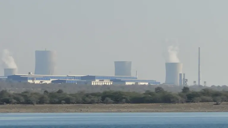

A semiconductor fab — short for fabrication facility — is the most complex factory humans have ever built. It is the site where slivers of silicon are transformed into the integrated circuits (ICs) that power every modern device, from smartphones and cars to satellites, missiles and AI data centres. A single state-of-the-art fab costs USD 15-20 billion, takes 3-5 years to construct, requires water purer than mineral water, dust levels 10,000 times cleaner than a hospital operating theatre, and a stable supply of high-skill engineers, gases and chemicals.
For decades India has been a world-class chip designer — over 20% of global VLSI design talent works for Indian arms of Intel, AMD, Nvidia, Qualcomm and others — but it has had zero commercial fabs. The India Semiconductor Mission (ISM) of 2021 aims to change that. For UPSC, this is a flagship GS III — Science & Technology, Economy and Internal Security topic.
What is a semiconductor — the underlying science
A semiconductor is a material whose electrical conductivity sits between that of conductors (copper, aluminium) and insulators (glass, rubber). Pure silicon is the workhorse of the industry; gallium arsenide, silicon carbide, gallium nitride and other compounds serve specialised needs.
The magic of semiconductors comes from doping — adding tiny amounts of impurities (phosphorus, boron) to silicon to create regions with excess electrons (n-type) or excess holes (p-type). A junction between n-type and p-type silicon is a diode; sandwich them and you get a transistor. Modern chips like Apple's M4 or Nvidia's Blackwell GPU pack over 200 billion transistors on a single die smaller than a thumbnail.
Why semiconductors matter
- Computing — every smartphone, laptop, server.
- Communications — 5G modems, optical transceivers.
- AI — GPUs, TPUs, custom AI accelerators.
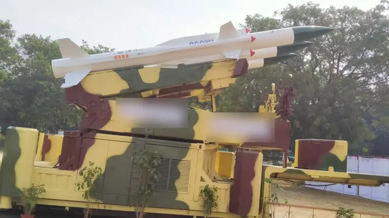
- Defence — radar, electronic warfare, missile guidance, satellites.
- Mobility — modern cars use 1,500-3,500 chips each.
- Strategic autonomy — chips are the new oil; whoever controls fabrication controls the digital economy.
The 2020-22 chip shortage during COVID, and the US-China tech war that followed, made every major economy realise that fab capacity is now a national-security asset.
How a fab works — chip-making 101
A modern logic chip is built up in 400-1,000 process steps over 8-12 weeks. The major stages:
- Wafer preparation — high-purity silicon ingots are sliced into 300 mm wafers polished to mirror flatness.
- Deposition — thin films of insulators and conductors are laid down using chemical vapour deposition (CVD) or atomic layer deposition (ALD).
- Photolithography — a circuit pattern is projected through a photomask onto a photosensitive resist layer using deep-UV (DUV) or extreme-UV (EUV) light. EUV systems cost USD 200-380 million each and are made only by ASML in the Netherlands.
- Etching — exposed resist is removed; underlying material is chemically or plasma-etched.
- Doping (ion implantation) — accelerated ions are blasted into silicon to create transistor regions.
- Metallisation — copper interconnects are deposited to wire transistors together; up to 15 metal layers.
- Testing — each die is electrically probed.
- Packaging (OSAT) — wafers are diced, dies are mounted in packages, wire-bonded, encapsulated and tested again. Outsourced Semiconductor Assembly and Test (OSAT) facilities do this and are far cheaper than full fabs.
Process nodes
The node (e.g., 28nm, 7nm, 3nm) loosely indicates transistor size — smaller nodes mean more transistors per chip and lower power per operation.
| Node | Used for | Status |
|---|---|---|
| 180nm-65nm | Power management, automotive, sensors | Mature; most demand stable |
| 28nm | Microcontrollers, ISP, automotive | Sweet spot for new entrants |
| 14nm-7nm | Mobile SoCs, mid-range CPUs | TSMC, Samsung, Intel |
| 5nm-3nm | Flagship phones, AI GPUs | TSMC dominant |
| 2nm and below | Next-gen AI, HPC | TSMC + Samsung + Intel race ongoing |
India's chip story — from BEL to ISM
India's first attempt at indigenous chip-making began with Semiconductor Complex Ltd (SCL), Mohali, set up in 1976. A 1989 fire crippled it; the facility today fabricates strategic chips for ISRO and DRDO at 180nm, but is far from commercial scale.
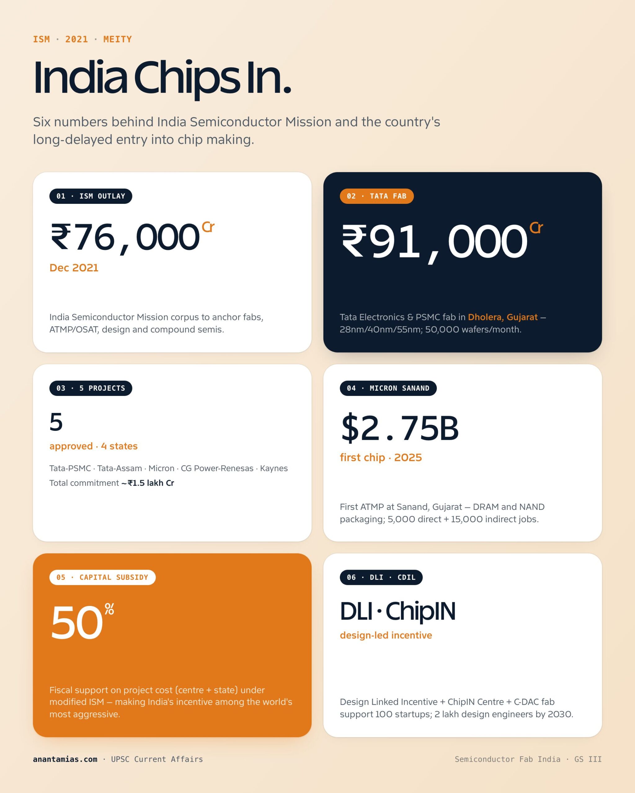
After three decades of false starts, the India Semiconductor Mission (ISM) was launched in December 2021 with an initial outlay of Rs 76,000 crore under MeitY. ISM offers up to 50% capital subsidy for fabs, OSATs, display fabs and compound-semiconductor units. The mission is anchored by Digital India Corporation.
Approved projects under ISM (as of 2025)
| Project | Location | Type | Status |
|---|---|---|---|
| Tata Electronics + PSMC fab | Dholera, Gujarat | 28nm logic + mature nodes | Construction underway; first wafers expected 2026 |
| Tata Semiconductor Assembly & Test | Jagiroad, Assam | OSAT | Construction underway |
| Micron OSAT | Sanand, Gujarat | DRAM/NAND ATMP | Phase 1 packaging from 2025 |
| CG Power + Renesas + Stars | Sanand, Gujarat | OSAT for automotive | Approved |
| Kaynes Semicon | Sanand, Gujarat | OSAT | Approved |
| HCL-Foxconn JV | Jewar, UP | OSAT/display drivers | Approved 2025 |
Cumulative committed investment across approved projects has crossed Rs 1.5 lakh crore. The Cabinet in September 2024 expanded ISM to a second tranche with fresh outlay; further expansion announced in 2025.
Allied initiatives
- Design-Linked Incentive (DLI) scheme — supports 100+ Indian fabless start-ups.
- Semicon India — annual flagship conference; Semicon India 2025 hosted in Greater Noida.
- Chips to Startup (C2S) programme — trains 85,000 engineers in VLSI/ESDM design across 113 institutions.
- National Centre for Excellence in Semiconductor (CoE-SC) at IIT Bombay and IIT Madras.
- PLI for IT Hardware 2.0 — anchors downstream demand.
- Critical Minerals Mission (2024) — secures gallium, germanium, rare earths needed for compound semiconductors.
Why India lacks fabs — the real challenges
| Challenge | Detail |
|---|---|
| Capital intensity | A single 28nm fab costs USD 5-7 billion; advanced nodes USD 15-20 billion |
| Long gestation | 3-5 years to build, another 1-2 to ramp; ROI horizon 10+ years |
| Talent depth | India has design talent but limited fab-floor process engineering |
| Supply chain | Ultra-pure water, gases, chemicals, masks, EUV systems all imported |
| Power and water | A modern fab consumes 100 MW+ continuous power and 10 million litres of ultra-pure water daily |
| IP and tech access | Cutting-edge process IP held by TSMC, Samsung, Intel; export controls (US, NL, JP) on EUV |
| Geopolitical risk | US-China decoupling; Taiwan Strait tensions affect entire supply chain |
| Demand certainty | Captive Indian demand for high-end chips remains modest vs global scale |
Global landscape
| Country/Region | Share of global fab capacity (approx.) | Strategic move |
|---|---|---|
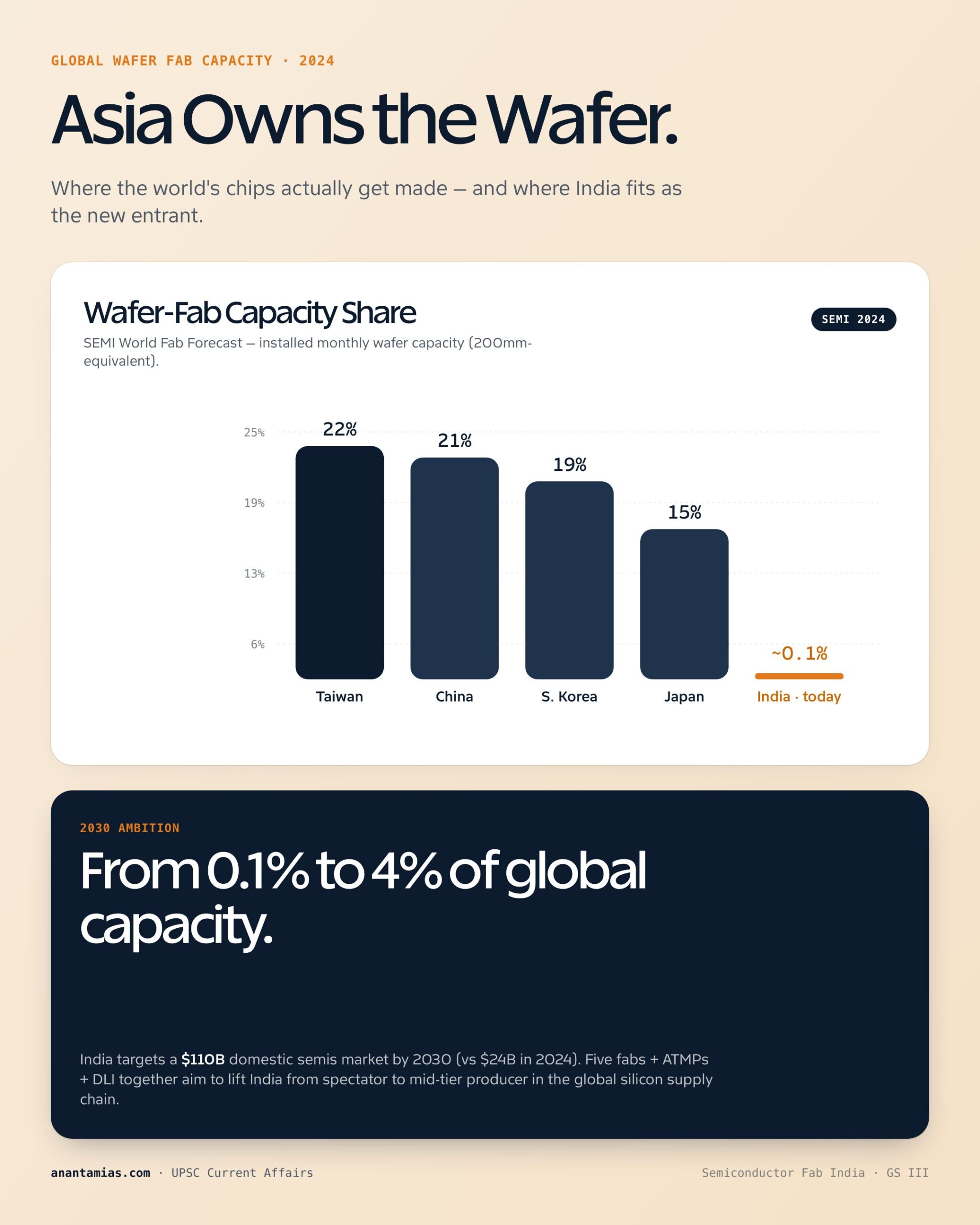
| Taiwan (TSMC) | ~22% | Dominates leading-edge logic; "silicon shield" |
| South Korea | ~21% | Memory leader (Samsung, SK Hynix) |
| China | ~19% | Massive subsidies; SMIC pushing 7nm despite sanctions |
| Japan | ~13% | Rapidus joint venture targeting 2nm |
| United States | ~10% | CHIPS and Science Act, USD 52 billion subsidy |
| EU | ~8% | EU Chips Act, EUR 43 billion |
| India | <1% (currently) | ISM scaling up |
The CHIPS and Science Act (2022), EU Chips Act (2023), Japan's Rapidus consortium and Korea's K-Chips Act all reflect a coordinated democratic-bloc effort to reduce dependence on Taiwan and East Asia. India's ISM is the South Asian piece of this jigsaw.
Recent developments (2024-26)
- Cabinet approved a second wave of ISM projects in 2024-25 including HCL-Foxconn at Jewar.
- Tata-PSMC Dholera fab broke ground in 2024; pilot wafers expected 2026.
- Micron Sanand packaging facility began trial production in 2024.
- India's first Made-in-India chip (a basic chip from Tata Assam) was unveiled in 2025 announcements.
- Semicon India 2024 and 2025 drew commitments from ASML, Applied Materials, Lam Research, KLA and Tokyo Electron.
- India-US iCET (Initiative on Critical and Emerging Technologies) and India-EU Trade and Technology Council identified semiconductors as a priority pillar.
- Quad Semiconductor Supply Chain Initiative mapped resilient supply routes.
- Critical and Strategic Minerals list (2023) and Mineral Auction Reforms opened up gallium, germanium, lithium and rare earth exploration.
- Indigenous SHAKTI processor (IIT Madras) and VEGA (CDAC) families progressing for sovereign computing.
- Bharat 6G Vision (2023) and National Quantum Mission (2023) create downstream demand for indigenous chips.
Way forward
- Stay the course on ISM — fabs need 10-year policy certainty.
- Anchor demand — government procurement of indigenous chips for railways, defence, BharatNet, e-governance.
- Build the middle — OSATs and 28-90nm specialty fabs first; aim for leading edge later.
- Talent pipeline — scale C2S to 200,000 engineers; create dedicated National Semiconductor Research Centre.
- Supply chain depth — incentivise photoresist, specialty gas, mask shop, equipment manufacturing.
- Power and water — dedicated semiconductor industrial parks with captive renewable power and zero-liquid-discharge water systems.
- Critical minerals — fast-track lithium, gallium, germanium, rare earth exploration via KABIL and ISM.
- Strategic partnerships — deepen iCET, Quad and India-Japan-Taiwan tech corridors.
- R&D in compound semiconductors — SiC, GaN for EVs, 5G, defence; less capital-intensive than silicon leading edge.
- Export-control regime — modernise SCOMET to align with Wassenaar/NSG counterparts.
Mains hook
"In a digitally networked world, fabrication of semiconductors is as strategic as oil refining was in the 20th century." Examine India's progress under the India Semiconductor Mission and the structural challenges that remain. (GS III, 250 words, 15 marks)
Prelims pointers
- India Semiconductor Mission (ISM) — launched December 2021 under MeitY; initial outlay Rs 76,000 crore.
- Approved fab — Tata Electronics + PSMC at Dholera, Gujarat (28nm and mature nodes).
- First OSATs — Micron at Sanand; Tata at Jagiroad, Assam.
- Design-Linked Incentive (DLI) — supports fabless chip start-ups.
- C2S programme — Chips to Startup, training VLSI engineers across 113 institutions.
- EUV lithography — made only by ASML (Netherlands).
- Major fab leaders — TSMC (Taiwan), Samsung (Korea), Intel (US).
- CHIPS and Science Act (US, 2022); EU Chips Act (2023); Rapidus (Japan, 2nm).
- Compound semiconductors — SiC, GaN; used in EVs, 5G, defence.
- SCL Mohali — India's legacy strategic fab under ISRO.
A semiconductor fab is not just a factory — it is a marker of where a country stands in the 21st-century technology hierarchy. India's bet on ISM is therefore both an industrial policy and a geopolitical statement, and the next five years will decide whether Dholera becomes the Hsinchu of South Asia or another cautionary tale.
Tell Google you want more of this.
Add Anantam IAS as a preferred sourceOne tap, and this site shows up more often in your own Top Stories, AI Overviews and AI Mode. Remove it any time.