Carbon is one of the most versatile elements in the periodic table. The same atom that builds the lead of a pencil also builds the diamond in a ring. The reason is that carbon’s four valence electrons can hybridise in several different ways, producing several different lattice structures with radically different properties. Two of those structures, graphene and carbon nanotubes, have transformed materials science over the past two decades. Both are made of pure carbon. Both have extraordinary mechanical, electrical, and thermal properties. Both have moved from laboratory curiosities to commercial products in a remarkably short time.
This article walks through what each material is, how they relate to one another, the key differences between them, the major applications, the safety questions, and the Indian research ecosystem that is contributing to the field. For UPSC GS-III the topic intersects nanotechnology, advanced manufacturing, materials science, and the broader story of indigenous research capacity. The Nobel Prize for graphene in 2010 to Andre Geim and Konstantin Novoselov turned the field from an academic specialty into a global research priority.
The Carbon Allotrope Family
Pure carbon exists in several distinct structural forms, called allotropes. Diamond is the cubic, three-dimensional lattice in which every carbon atom is bonded to four neighbours in a tetrahedral arrangement. Graphite is the layered structure in which carbon atoms form flat hexagonal sheets that stack loosely on top of each other. Charcoal and amorphous carbon are disordered packings of carbon. The newer allotropes, discovered or isolated only in the last few decades, include graphene as a single layer of the graphite sheet, carbon nanotubes as rolled-up versions of that sheet, fullerenes as closed cage molecules including the famous buckminsterfullerene, and graphdiyne as an experimental 2D variant with alternating single and triple bonds.
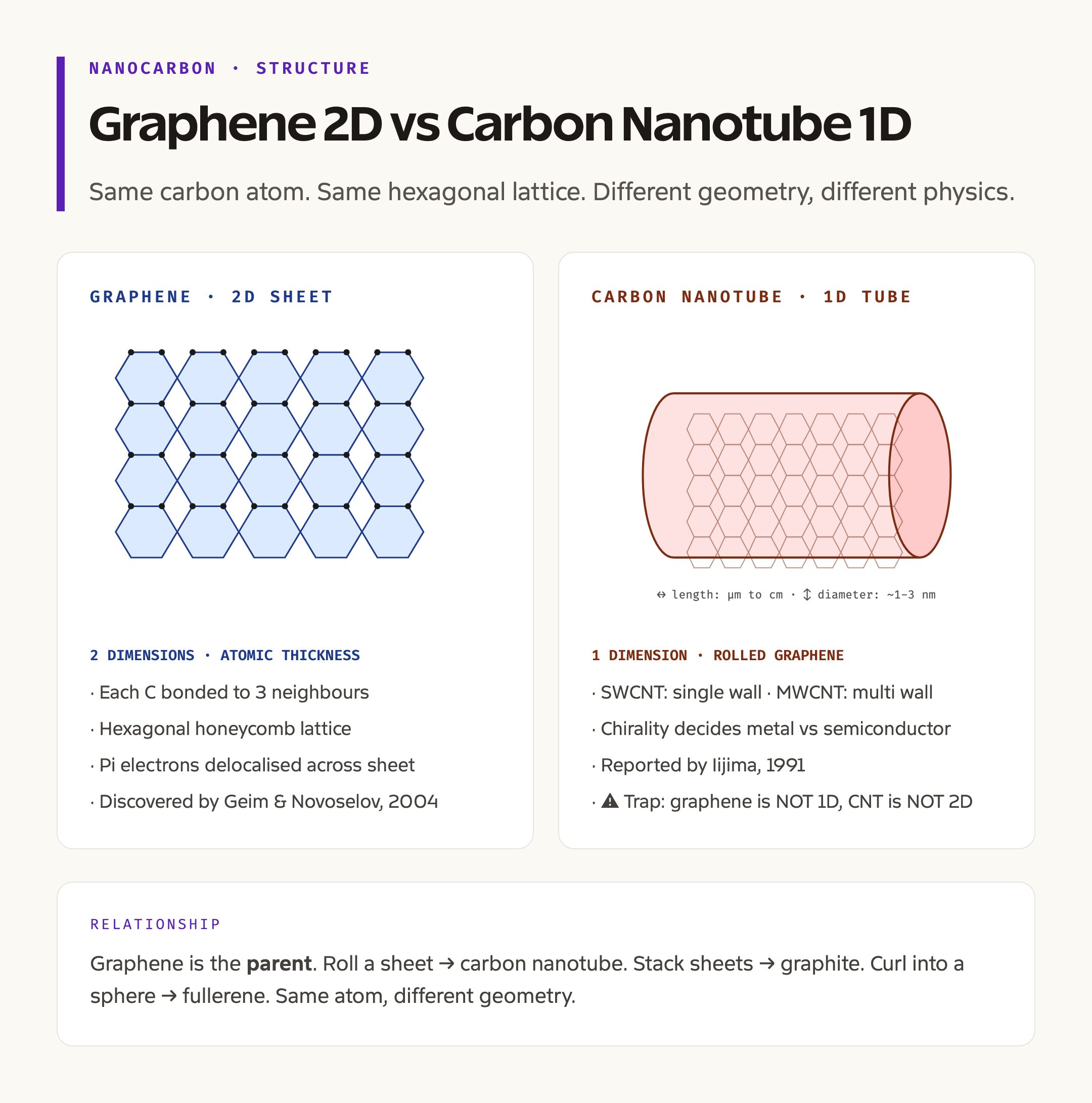
Graphene is the parent of the modern allotrope family. Once you have an isolated 2D graphene sheet, you can roll it into a tube to get a carbon nanotube, you can stack it back into thick layers to get graphite, you can curl it into a sphere to get a fullerene, and you can chemically modify it to get a wide range of derivatives. Understanding graphene is therefore the entry point to the entire nanocarbon field.
What Graphene Is
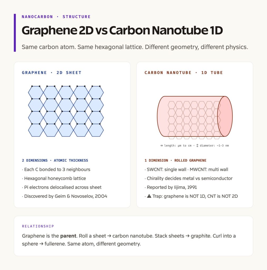
Graphene is a single layer of carbon atoms arranged in a hexagonal honeycomb lattice. Each carbon atom is bonded to three neighbours through strong sigma bonds at 120-degree angles, with the fourth valence electron delocalised in a pi orbital that extends across the whole sheet. The strong in-plane bonding gives graphene its mechanical strength. The delocalised pi electrons give it remarkable electrical conductivity. The two-dimensional structure gives it a unique set of electronic and thermal properties that have no analogue in conventional materials.
Graphene was first isolated in 2004 by Andre Geim and Konstantin Novoselov at the University of Manchester, using the now-famous adhesive-tape method to peel single layers from a graphite block. They received the Nobel Prize in Physics in 2010 for the discovery. Production methods have since matured, with chemical vapour deposition on copper foil being the standard for high-quality films, liquid-phase exfoliation for industrial-scale flakes, and reduced graphene oxide for cheaper bulk applications.
What Carbon Nanotubes Are
A carbon nanotube is a graphene sheet rolled up into a cylinder. The rolled tube has a diameter on the order of one to a few nanometres and a length that can range from microns to centimetres. The way the sheet is rolled, captured by a pair of integers called the chirality indices, determines whether the resulting tube behaves as a metal or as a semiconductor. The metallic variant carries current with negligible resistance. The semiconducting variant has a band gap that can be tuned by choosing the chirality, opening the door to nanotube transistors and integrated circuits.
Single-walled carbon nanotubes, abbreviated SWCNTs, consist of one rolled-up graphene sheet. Multi-walled carbon nanotubes, abbreviated MWCNTs, consist of multiple concentric tubes nested inside one another, somewhat like a Russian doll. SWCNTs are harder to make in pure form but have cleaner electronic properties. MWCNTs are easier to manufacture in bulk and are used in mechanical and conductive composite applications.
Carbon nanotubes were systematically reported in 1991 by Sumio Iijima, though earlier observations exist. The discovery slightly preceded the isolation of graphene, but the conceptual relationship between the two has come into sharp focus only since 2004.
Structural Comparison: 1D vs 2D
A graphene sheet is two-dimensional. It has length and width that can extend to centimetres, but its thickness is the diameter of a single carbon atom. A carbon nanotube is one-dimensional. It has length that can extend to millimetres but a width that is fixed at a few nanometres. The dimensional contrast is the most fundamental difference between the two materials. Graphene behaves as a flat conductor with carriers free to move in two directions. CNTs behave as quasi-one-dimensional conductors with carriers confined along the tube axis.
A common prelims trap is the inversion of these dimensions. The factually correct statement is that graphene is a 2D sheet and CNTs are 1D tubes. Any statement to the contrary is wrong.
Mechanical Properties
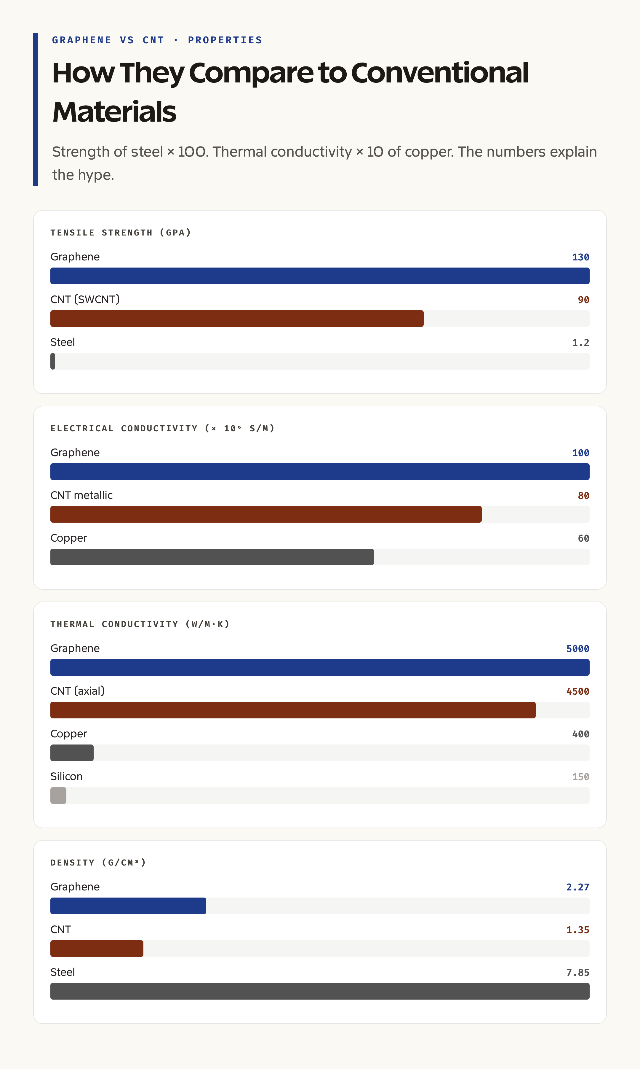
Graphene is the strongest material ever measured. Its tensile strength, the force per unit cross-sectional area required to break the lattice, is about 130 gigapascals, more than 100 times greater than steel of equivalent weight. Its Young’s modulus, a measure of stiffness, is about 1 terapascal. The combination makes graphene effectively unbreakable in pure form, though defects, edges, and grain boundaries reduce the practical strength of large-area samples.
Carbon nanotubes are slightly less strong than perfect graphene because the rolling introduces curvature stresses, but they are still remarkably tough. Their tensile strength is in the range of 60 to 100 gigapascals depending on the specific tube. Their cylindrical geometry makes them excellent reinforcement fibres in composite materials. A small percentage of CNT loading in a polymer or metal matrix can dramatically increase strength, stiffness, and impact resistance.
The implication is that graphene is the strongest single sheet in nature, while CNTs are the strongest fibre. Both belong in any future materials roadmap for aerospace, ballistic protection, and high-performance structural composites.
Electrical Properties
Graphene has a zero band gap. It is neither a pure conductor nor a pure semiconductor, but a semimetal where the valence and conduction bands meet at a single point in momentum space. Charge carriers move through graphene as if they were massless particles, and electron mobilities exceed those of any other known material. The catch is that the zero band gap makes graphene difficult to use as a transistor switch, because the device cannot be turned off cleanly. Significant research effort is devoted to opening a band gap in graphene through nanoribbon patterning, doping, or stacking.
Carbon nanotubes can be either metallic or semiconducting depending on chirality. About one-third of randomly grown CNTs are metallic and two-thirds are semiconducting. The semiconducting tubes have a band gap that depends on the tube diameter, with smaller tubes having larger gaps. Pure semiconducting CNTs make excellent transistors and have been demonstrated in working integrated circuits, including a complete RISC-V processor in 2019. Whether CNTs displace silicon at the leading edge of angstrom-scale chip manufacturing is one of the open questions in semiconductor technology.
Thermal Properties
Graphene is one of the best thermal conductors known. Its in-plane thermal conductivity exceeds 4,000 to 5,000 watts per metre kelvin, more than ten times that of copper. The high conductivity makes graphene an attractive thermal management material for electronics, where heat removal is increasingly the limiting factor in device performance.
Carbon nanotubes have similarly high thermal conductivity along the tube axis, on the order of 3,000 to 6,000 watts per metre kelvin for individual tubes. The conductivity drops sharply across tubes, so a bulk CNT mat is much less conductive than a single tube. Both materials are used as thermal interface materials in high-performance computing and power electronics applications.
Applications
Graphene applications span energy storage, electronics, composites, and biomedicine. Graphene-enhanced lithium-ion batteries achieve faster charging and longer cycle life. Supercapacitor electrodes made of graphene have very high specific capacitance. Graphene oxide membranes are used in water purification, particularly for desalination and for the removal of micropollutants. Graphene composites in concrete improve mechanical strength and reduce cement consumption. Graphene-based biosensors detect glucose, viral antigens, and DNA at very low concentrations.
Carbon nanotube applications cluster around composites, electronics, and electrochemistry. CNT-reinforced polymer composites appear in aerospace structural panels, sporting goods, and automotive parts. CNT-based field emission displays were an early commercial application. CNT-based transistors are progressing through laboratory demonstrations toward small-volume commercial use. CNT yarns and fibres can carry currents at densities that would melt copper, opening applications in lightweight power transmission and electromechanical actuators.
For the broader nanotechnology context, see the article on nanotechnology and on quantum dots.
Safety and Toxicology
A common prelims trap is the claim that CNTs are biodegradable and safe for human consumption. This is false. Carbon nanotubes, like asbestos fibres, are needle-shaped at the nanoscale. Inhaled CNT dust can lodge in lung tissue and cause inflammation, fibrosis, and in animal studies, mesothelioma-like lesions. Industrial handling of CNTs requires occupational health protection comparable to that for asbestos. Environmental release of CNTs from waste streams is a separate concern, and disposal protocols are still being standardised.
Graphene is somewhat less hazardous than CNTs because it is a flat sheet rather than a needle, but graphene oxide and other functionalised derivatives can also produce inflammatory responses. Toxicology research on both materials is active, and the European Union’s REACH framework now treats them as substances requiring registration above specified production thresholds. India’s regulatory framework for nanomaterials is at an earlier stage, with the Department of Science and Technology and the Bureau of Indian Standards developing guidelines.
The Indian Research Ecosystem
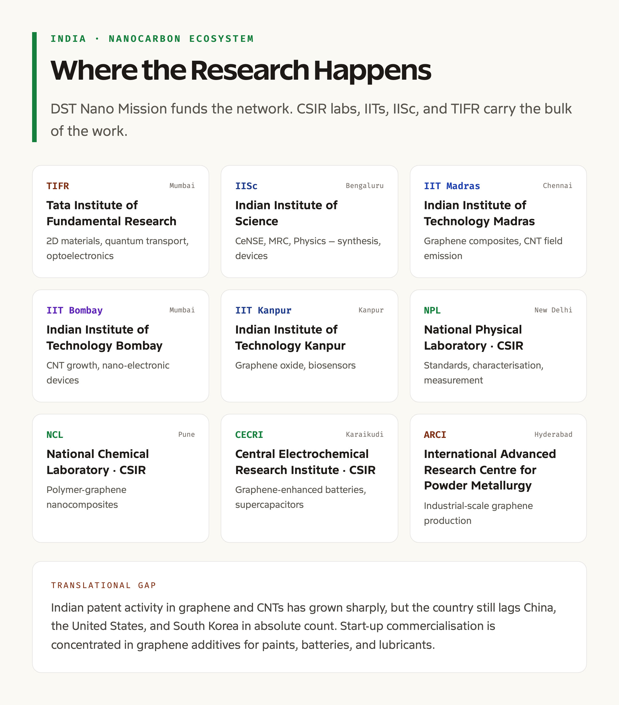
India has a strong research base in nanocarbon. The Tata Institute of Fundamental Research in Mumbai runs significant graphene and 2D materials groups working on quantum transport, optoelectronics, and topological matter. The Indian Institute of Science in Bengaluru has multiple groups across the Department of Materials Engineering, the Centre for Nano Science and Engineering, and the Department of Physics covering synthesis, characterisation, and devices. The Indian Institutes of Technology, particularly Madras, Bombay, Kanpur, Delhi, Kharagpur, and Roorkee, run substantial nanotechnology programmes.
The CSIR network adds the National Physical Laboratory in New Delhi, the National Chemical Laboratory in Pune, the Central Electrochemical Research Institute in Karaikudi, and several others. The Department of Science and Technology runs the Nano Mission as a coordinating umbrella for nanotechnology funding, with successive phases dedicated to research grants, infrastructure, and translational projects. Indian patent activity in graphene and CNTs has grown sharply, though the country still lags China, the United States, and South Korea in absolute count.
The translational gap between research and commercial product is the standard Indian story. A handful of start-ups, mostly attached to academic spin-offs, are commercialising graphene additives for paints, batteries, and lubricants. The defence research establishment is funding selected nanocomposite work for armour and stealth applications.
What is Next
Both graphene and CNTs are now in their second decade as research priorities. The next decade will be defined by manufacturing scale-up. Producing wafer-scale graphene films of consistent quality, sorting CNTs by chirality at industrial volumes, and integrating both materials with conventional silicon, polymer, and metal processes are the engineering bottlenecks. Several adjacent 2D materials, including molybdenum disulphide, hexagonal boron nitride, and the broader transition-metal dichalcogenide family, are being studied alongside graphene because they offer band gaps and other properties that graphene lacks.
The longer horizon includes graphene-based quantum devices, CNT integrated circuits replacing silicon at advanced nodes, and a wide range of energy and biomedical applications that cannot proceed without the new materials. The intersection with nanomedicine and with the broader bet on advanced materials is increasingly clear.
Prelims and Mains Pointers
For prelims, the high-yield facts are that graphene is a 2D single-layer carbon sheet and CNTs are 1D rolled-up tubes, that graphene is the strongest material known, that graphene has zero band gap while CNTs can be either metallic or semiconducting, that the 2010 Physics Nobel Prize went to Geim and Novoselov for graphene, and that CNTs are not biodegradable or safe for human consumption.
For mains, the relevant arguments are about the role of advanced materials in industrial competitiveness, the structure of the Indian research ecosystem, and the regulatory framework for nanomaterials. Both graphene and CNTs are platform technologies whose impact will be felt in dozens of downstream industries over the coming decades, and a working command of their properties is necessary for any GS-III answer on materials science or nanotechnology.
Tell Google you want more of this.
Add Anantam IAS as a preferred sourceOne tap, and this site shows up more often in your own Top Stories, AI Overviews and AI Mode. Remove it any time.