
The semiconductor industry just spent the last decade arguing about whether Moore’s Law was dead. While that argument was happening, a quieter shift was unfolding in research labs from MIT to IISc to TSMC’s R&D wing. Researchers were moving past the silicon era altogether and asking what transistors built from atomically thin 2D materials might look like. Those questions have produced the technology we now call angstrom-scale chips, and the early demonstrations are reshaping what “advanced node” means.
An angstrom is one ten-billionth of a meter, ten times smaller than a nanometer. When chip industry insiders talk about angstrom-scale chips, they’re describing devices where critical features, channel thickness, gate length, and dielectric layers, are measured in single atoms or fractions of nanometers. To get there, you can’t just shrink silicon. You have to switch material systems. That’s where graphene, molybdenum disulfide, hexagonal boron nitride, and other 2D materials enter the story.
For India, this is more than a science update. The India Semiconductor Mission has been built on the assumption that India can climb the value chain by entering the global semiconductor industry now. Angstrom-scale technology changes the slope of that climb. The country needs a clear-eyed read on where this generation of chips is going, what it requires, and where India can plausibly play.
Quick Facts at a Glance
- Definition: Chips with critical dimensions measured in angstroms (1 angstrom = 0.1 nanometer = 10^-10 meter)
- Materials: 2D materials including graphene, molybdenum disulfide (MoS2), tungsten diselenide (WSe2), hexagonal boron nitride (hBN)
- Why beyond silicon: At sub-2nm scales, silicon’s electron mobility drops, leakage current rises, and quantum effects break classical transistor behavior
- Current commercial frontier: TSMC, Samsung, and Intel are at 2nm/3nm nodes (2026)
- Key advantages of 2D materials: Atomic thickness, high carrier mobility, low leakage, enables true gate-all-around scaling
- India’s frame: India Semiconductor Mission 2.0 expected to fund design, fab, and ATMP, with research push for post-silicon technologies
Why in News: A Generational Shift in Chip R&D
In late April 2026, multiple research groups including teams associated with MIT, IBM Research, TSMC, and Indian institutes including IIT Bombay and IISc, reported coordinated progress on transistor structures using 2D materials at sub-nanometer feature sizes. Several papers and industry statements positioned these as the first credible demonstrations of devices that work at angstrom-scale dimensions while meeting basic switching, mobility, and reliability targets.
This isn’t a single product launch. It’s a research-to-roadmap moment. The next decade of advanced semiconductor nodes is going to be defined by how fast 2D materials, new dielectrics, new contact metals, and new lithography techniques can be put together in commercial fabs. India’s policy community is paying attention because the country’s semiconductor strategy is being shaped now, and the underlying technology base is shifting under it.
Background and Historical Context
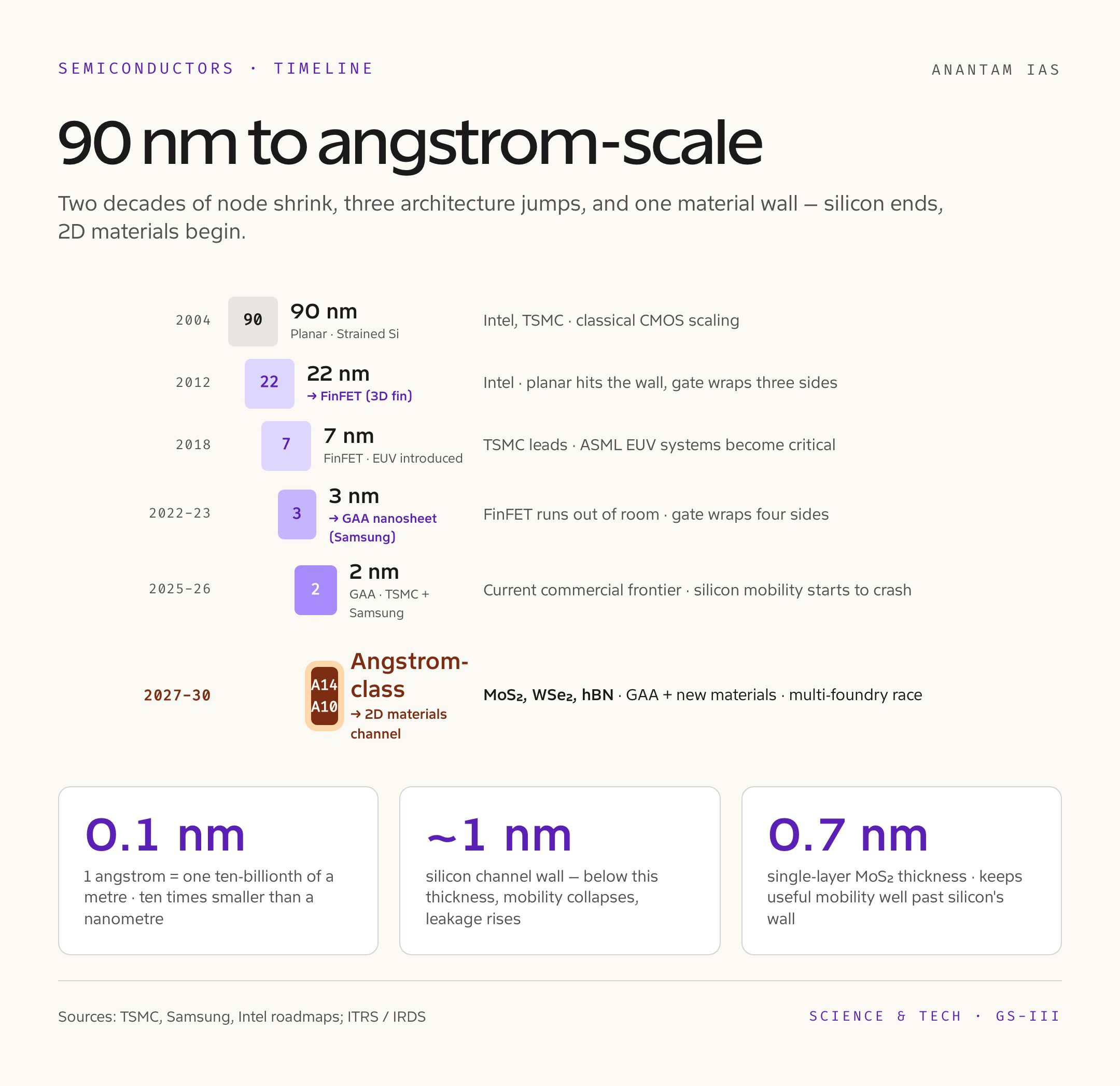
Moore’s Law, formulated by Gordon Moore in 1965 and refined in 1975, predicted that the number of transistors on a chip would roughly double every two years. For five decades, the industry held to that pace through ever-finer lithography, materials innovation, and architectural creativity. Each “node” became shorthand for a generation: 90nm, 65nm, 45nm, 32nm, 22nm, 14nm, 10nm, 7nm, 5nm, 3nm, and now 2nm.
Around the 22nm to 14nm transition, the planar transistor architecture hit physical limits. Intel’s introduction of FinFET (3D fin-shaped transistor channel) extended the curve. Around 3nm, FinFET also ran out of room, and the industry moved to gate-all-around (GAA) architectures, where the gate wraps the channel from all sides. Samsung was first to commercial GAA at 3nm, followed by TSMC at 2nm.
But GAA on silicon is only a partial answer. Silicon’s intrinsic properties limit how thin a channel can be before electron mobility collapses. Below roughly 1nm channel thickness, silicon stops being a useful semiconductor. That’s the wall.
2D materials were always the candidate for the post-silicon era. Graphene was isolated by Geim and Novoselov in 2004 (Nobel Prize 2010). Molybdenum disulfide became a serious electronic material in the 2010s. Hexagonal boron nitride emerged as the gate dielectric pair for these materials. The challenge for two decades has been engineering: making large-area, defect-free 2D layers, integrating them into existing fab flows, and solving contact resistance with metals.
If you’re tracking the broader semiconductor and material science arc, our explainers on graphene, semiconductor fab, and Silicon Valley of India are good companion reads.
How It Works: From Silicon FinFETs to 2D Channels
A transistor is a switch. It uses a control voltage on a “gate” to turn current on or off through a “channel” between source and drain electrodes. The smaller and more controllable the channel, the more transistors fit in a given area, and the more efficient each switching event becomes.
In a silicon FinFET, the channel is a thin vertical fin of silicon, with the gate wrapping three sides. In a GAA transistor, the channel is a stack of nanosheets, with the gate wrapping all four sides. In a 2D-material transistor, the channel is one or a few atomic layers of a material like MoS2, with gates above and below and ultra-thin hBN dielectrics separating them.
The advantages of 2D channels:
- Atomic thinness. Single-layer MoS2 is about 0.7nm thick, well below the silicon wall.
- No dangling bonds. 2D materials have all their bonds in-plane, reducing surface scattering of electrons.
- High mobility at thinness. Silicon mobility crashes when thinned. MoS2, WSe2, and others retain useful mobility at one-atom thickness.
- Low leakage. Atomic thinness means precise control by the gate, with very little off-state current.
- Heterostructure flexibility. 2D materials stack like Lego, allowing custom electronic properties not accessible in 3D crystals.
The challenges:
- Wafer-scale growth. Producing 12-inch wafers of single-crystal MoS2 with controlled orientation is hard.
- Contact resistance. Metal-to-2D contacts have high resistance unless engineered with specific interface chemistry.
- Process compatibility. Existing fab processes are silicon-tuned. Integrating 2D materials needs new tools and new flows.
- Reliability. Long-term stability under switching stress is still being validated.
- EUV lithography requirements. Patterning angstrom-scale features needs the most advanced lithography in the world, currently dominated by ASML’s EUV systems.
Why It Matters: Five Strategic Threads

One, computing economics. Every modern frontier, AI, edge computing, autonomous systems, depends on cheap, fast, low-power chips. Angstrom-scale technology determines whether the next decade gets another order of magnitude in capability or stalls.
Two, supply chain leverage. Whoever masters angstrom-scale fabrication holds enormous geopolitical leverage. The current concentration in Taiwan, South Korea, and the Netherlands (ASML) is already a security concern globally. A new technology generation reshuffles who has what.
Three, energy efficiency. Data centers already consume meaningful national-grid percentages. AI workloads are growing 5-10x annually. More efficient chips are the only way to keep that curve sustainable.
Four, India’s window. India’s semiconductor entry is happening at a moment when the technology base is shifting. If India focuses purely on legacy nodes (28nm and above) for fabs, it builds capability for an industry that’s increasingly commoditized. If India invests in research and design at the angstrom-scale frontier, it can leapfrog into higher-value segments.
Five, defense and dual-use. Advanced chips power radar, missile guidance, satellite payloads, and quantum sensors. National security at chip-level resolution is now part of the strategic conversation.
Detailed Analysis
India Semiconductor Mission and Where Angstrom-Scale Fits
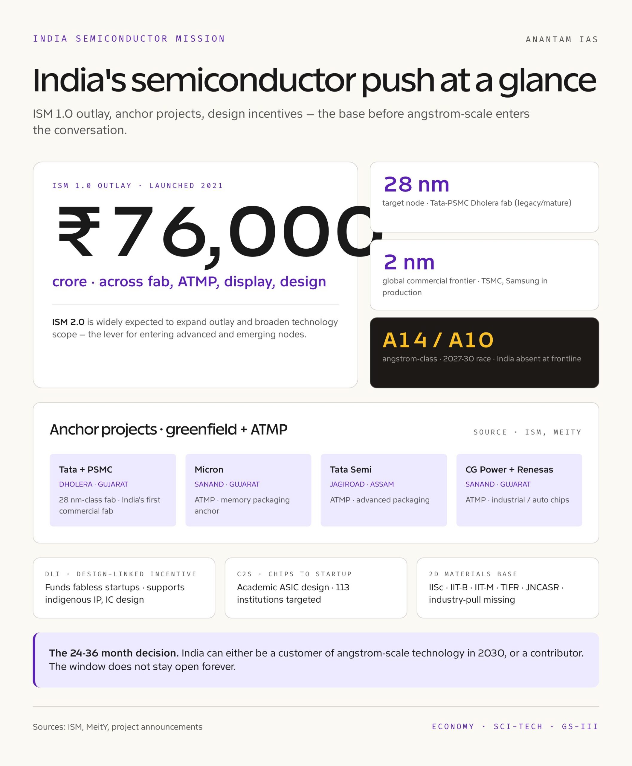
India Semiconductor Mission (ISM) was launched in 2021 with a 76,000 crore rupees outlay across fab, ATMP (assembly, testing, marking, packaging), display fab, and design-linked incentives. ISM 2.0 is widely expected to expand the outlay and broaden the technology scope. The current Indian fab investments, Tata Electronics with PSMC at Dholera (28nm class), Micron at Sanand (ATMP), Tata Semiconductor at Jagiroad (Assam, ATMP), CG Power with Renesas, target legacy and mature nodes.
That’s the right starting point. You don’t begin with 2nm. But India also needs a parallel research and design push for advanced and emerging technologies. The Design-Linked Incentive (DLI) scheme supports fabless startups, and the Chips to Startup (C2S) program funds academic ASIC design. What’s missing in scale is a focused 2D materials and angstrom-scale device research program tied to industry pull.
The IISc nano-electronics center, IIT Bombay’s nanofabrication facility, and SCL Mohali have research-grade capability. Linking them to an explicit angstrom-scale roadmap, with industry partnership and funded talent pipelines, is the next logical step.
TSMC, Samsung, Intel, and the Race
TSMC remains the global leader, with 2nm in production by late 2025 and active research on 1nm-class and angstrom-scale equivalents (TSMC uses “A14” and “A10” naming conventions for angstrom-class technology). Samsung is competing closely. Intel, after years behind, is pushing to regain leadership through Intel Foundry, with 18A and 14A nodes targeted by mid-decade. China’s SMIC is operating at 7nm class through workarounds but constrained by US export controls on EUV lithography.
The competitive position depends on three things: lithography (ASML EUV and high-NA EUV), materials engineering, and design talent. India is currently absent from frontline fab competition but has strong design talent and growing materials research.
The 2D Materials Ecosystem in India
Indian institutions have a credible 2D materials base. IISc Bengaluru, IIT Bombay, IIT Madras, IIT Delhi, JNCASR, and TIFR have published widely on graphene, MoS2, WSe2, and heterostructures. Industry participation has been thinner. Linking academic research to fab-relevant validation is the gap NIPCR-style infrastructure could partly address, except in the chip domain rather than pharma.
For policy context, our piece on national IPR policy explains the broader IP environment in which Indian chip and materials innovation must operate.
Comparative Perspective
| Generation | Year | Architecture | Channel Material | Lead Foundry |
|---|---|---|---|---|
| 90nm | 2004 | Planar | Strained Si | Intel, TSMC |
| 22nm | 2012 | FinFET | Strained Si | Intel |
| 7nm | 2018 | FinFET | Si | TSMC |
| 3nm | 2022-23 | FinFET (TSMC), GAA (Samsung) | Si | TSMC, Samsung |
| 2nm | 2025-26 | GAA nanosheet | Si | TSMC, Samsung |
| A14/A10 (angstrom-class) | 2027-30 (projected) | GAA + new materials | 2D materials emerging | Multi-foundry race |
The transition from “nm” to “angstrom” naming is partly marketing. TSMC’s “A14” is roughly equivalent to what would have been called 1.4nm under earlier conventions. The substantive shift is in materials and architecture, not in feature shrink alone.
Challenges and Critiques
The technology is real, the deployment is hard.
Manufacturability. Lab demonstration to high-volume manufacturing is a 5-10 year journey for any new transistor technology. 2D materials are still in early stages of that transition.
EUV access. High-NA EUV systems cost over $400 million each. Only ASML makes them. Export controls and supply constraints make access a strategic question.
Cost. Each new node has been more expensive than the last. Angstrom-scale wafers may cost more than $20,000 per wafer, restricting customer base to AI and high-end mobile.
Defects and yield. 2D materials have unique defect types. Achieving the parts-per-billion defect rates needed for commercial chip yields is unsolved at scale.
Talent shortage. The world has a few thousand people who can design at frontier nodes. India has a fraction of that. Building the talent pipeline takes a generation.
India’s bandwidth. The country can’t do everything. Spreading thin across legacy fabs, advanced design, materials research, packaging, and EDA risks not winning anywhere.
UPSC Prelims Pointers
- 1 angstrom = 0.1 nanometer = 10^-10 meter
- Moore’s Law was formulated by Gordon Moore in 1965 and predicts roughly doubling of transistors every two years
- Graphene was isolated by Andre Geim and Konstantin Novoselov in 2004; they won the Nobel Prize in Physics in 2010
- 2D materials include graphene (carbon), molybdenum disulfide (MoS2), tungsten diselenide (WSe2), and hexagonal boron nitride (hBN)
- Modern transistor architectures: planar, FinFET (3D fin), GAA (gate-all-around nanosheet)
- India Semiconductor Mission was launched in 2021 with a 76,000 crore rupees outlay
- Major Indian semiconductor projects: Tata-PSMC at Dholera (Gujarat), Micron at Sanand (Gujarat), Tata at Jagiroad (Assam)
- ASML (Netherlands) is the sole supplier of EUV lithography systems globally
- TSMC (Taiwan), Samsung (South Korea), and Intel (USA) are the leading advanced-node foundries
Mains Practice Questions
- GS Paper III: Explain the concept of angstrom-scale chips and discuss the role of 2D materials in extending Moore’s Law. What is the strategic significance for India? (250 words)
- GS Paper III: Evaluate India Semiconductor Mission against the backdrop of global advanced-node competition. Should India focus on legacy fabs, design, or research at the frontier? (250 words)
- GS Paper III: “Semiconductors are the new oil.” Discuss the geopolitical implications of advanced chip technology for India’s economic and security strategy. (150 words)
- GS Paper III: Analyze the role of 2D materials in next-generation electronics. How can India build domestic capability in this emerging field? (250 words)
Way Forward
India’s semiconductor strategy is correctly weighted toward fabs, ATMP, and design today. The next layer of strategy needs to add explicit angstrom-scale and 2D materials research with industry pull. That means a national 2D materials mission housed at an institution like IISc or a new dedicated center, with funded industry consortia. It means scaling up nanofabrication facilities at IITs and IISc to GLP-equivalent process discipline so that academic device demonstrations translate to fab roadmaps. It means design-linked incentives for chip startups working on emerging architectures, neuromorphic, in-memory computing, photonic, that are natural fits for 2D materials. And it means strategic alignment with partners (US, Japan, EU, Australia) on the materials, equipment, and IP needed to participate at the frontier.
The window for India to enter the next chip generation isn’t open forever. The decisions made over the next 24 to 36 months will determine whether the country is a customer of angstrom-scale technology in 2030 or a contributor to it.
Frequently Asked Questions
What are angstrom-scale chips?
Angstrom-scale chips are next-generation semiconductors with critical features measured in angstroms (one ten-billionth of a meter), using 2D materials like graphene and MoS2 instead of conventional silicon channels.
How are angstrom-scale chips different from 2nm chips?
2nm chips use silicon channels in gate-all-around architectures. Angstrom-scale chips push beyond silicon’s intrinsic limits using single-atom-thick 2D materials, achieving smaller features and lower leakage.
What is Moore’s Law?
Moore’s Law is the observation, formulated by Gordon Moore in 1965, that the number of transistors on a chip roughly doubles every two years. It has guided semiconductor scaling for five decades.
Why are 2D materials important for semiconductors?
2D materials like graphene and MoS2 are atomically thin, have high carrier mobility, low leakage, and stack into custom heterostructures. These properties enable transistors smaller than silicon allows.
Where does India stand in the semiconductor race?
India is building legacy and mature node fabs through India Semiconductor Mission, has a strong chip design talent base, and growing 2D materials research. It is not yet a frontier-node manufacturer.
What is the India Semiconductor Mission?
ISM is a 76,000 crore rupees national program launched in 2021 to support fabs, ATMP, display fabs, and design-linked incentives. ISM 2.0 is expected to expand scope and outlay.
What role does graphene play in angstrom-scale chips?
Graphene is one of several 2D materials studied for angstrom-scale transistors. It has very high carrier mobility but lacks a natural bandgap, so MoS2 and other transition metal dichalcogenides are often used as channel materials with graphene in supporting roles.
Will angstrom-scale chips reach consumer devices?
Yes, eventually. The first applications will likely be high-end AI accelerators and flagship mobile processors, before the technology percolates down to mainstream consumer chips later in the decade.
Tell Google you want more of this.
Add Anantam IAS as a preferred sourceOne tap, and this site shows up more often in your own Top Stories, AI Overviews and AI Mode. Remove it any time.