
Why in News?
On November 4, PIB reported that JNCASR researchers demonstrated terahertz data transmission across engineered barriers in a silicon photonic chip, offering a possible building block for future communication circuits.
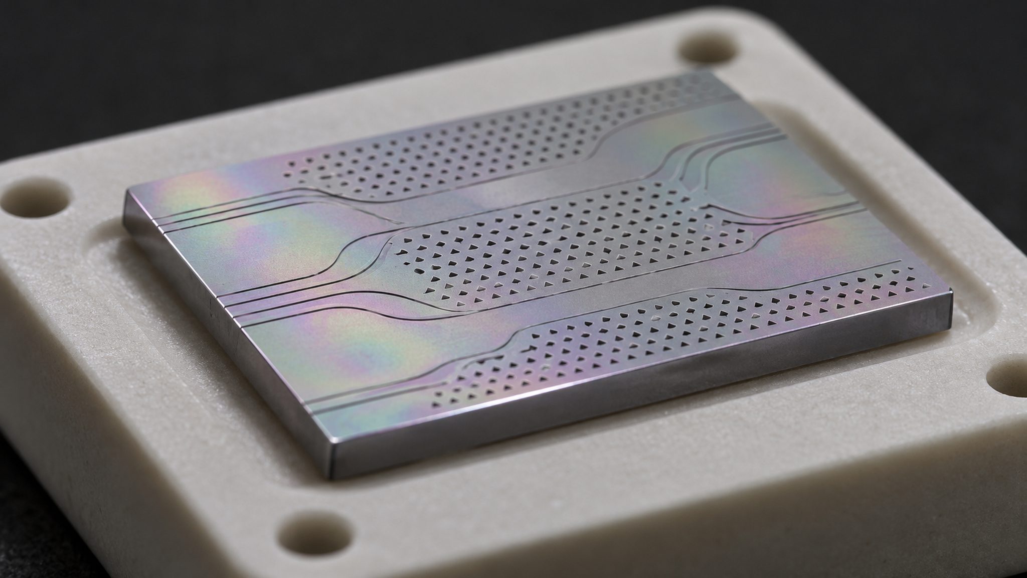
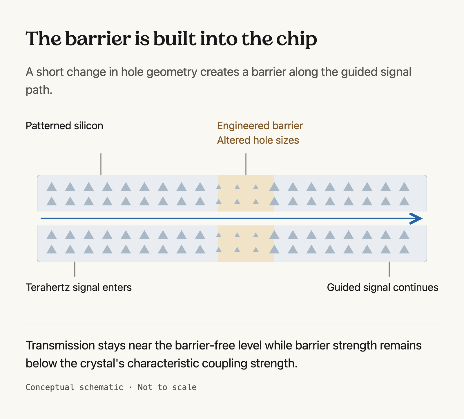
- The silicon photonic crystal uses patterned triangular holes to guide waves along a boundary between two regions; changing hole sizes creates the barrier under study.
- Measurements covered 310–360 GHz, while the power splitter demonstrated data transmission at 100 Gbit/s; that rate should not be assigned to every tested device.
- Transmission remained near its barrier-free level when barrier strength stayed below the crystal’s characteristic coupling strength, making the geometry and operating conditions central to the result.
- The work remains a laboratory demonstration. Electrical, thermal or mechanical tuning is a proposed next step rather than a capability already established in this release.
- Compact communication circuits need to route signals through bends and junctions without excessive loss; high-frequency bandwidth alone cannot solve that physical engineering problem.
- Device research contributes to future networks alongside spectrum decisions, interoperability and 6G standards and security policy.
UPSC Relevance
Prelims Relevance
- Terahertz frequencies: electromagnetic frequencies between microwave and infrared regions.
- Photonic crystal: a patterned structure that controls the propagation of electromagnetic waves.
- Backscattering: signal energy redirected toward the incoming path.
- Waveguide: a structure that channels electromagnetic waves along a chosen route.
- QAM: modulation that encodes information through amplitude and phase.
Mains Relevance
GS Paper 3
- Indigenous research: translating laboratory photonic devices into reliable communication components.
- Technology assessment: separating a demonstrated mechanism from commercial readiness and network deployment.
Essay
- Scientific progress: useful innovation combines a new principle with evidence about where it works.
Background and Context
Why Terahertz Circuits Need Better Waveguides
A communication signal must survive the path through a circuit before its available bandwidth can become useful data capacity.
- Terahertz waves occupy a high-frequency part of the electromagnetic spectrum. Their broad potential bandwidth makes them attractive for future communications, but the useful capacity depends on devices that generate, guide and detect them.
- Waveguides channel waves through a designed route. A sharp bend, junction or sudden structural change can reflect or scatter energy, leaving less of the original signal available at the intended output.
- Photonic crystals control propagation through their spatial pattern. Here, triangular holes in silicon form a honeycomb-like arrangement; changing the pattern changes the electromagnetic environment experienced by the travelling wave.
- Boundary channels guide waves between two differently arranged regions. Their resistance to certain backscattering processes is useful, but it must be tested for the particular obstacles a practical circuit will contain.
- Chip design shapes a device’s function as well as its material. The broader distinction between a specialised component and a complete system also appears in application-specific vision processors.
What the Engineered Barrier Demonstrates
The obstacle is a deliberately altered section of the chip’s hole pattern, and its effect depends on the surrounding crystal.
- Barrier geometry was introduced by changing triangular-hole sizes over a short waveguide section. This is a controlled alteration of the circuit itself, rather than a test of transmission through buildings or other everyday objects.
- Transmission stayed close to the barrier-free case below a characteristic coupling threshold. The condition matters: an obstacle cannot be assumed harmless regardless of its geometry, strength or relationship to the guiding structure.
- Three layouts tested the concept: sequential barriers, a bent route with a central barrier and a splitter with a barrier in one branch. Together, they examined routing situations beyond one straight channel.
- The splitter produced nearly identical output signals despite the barrier in one branch. Its high-speed test used QAM, which carries information through changes in signal amplitude and phase.
- The comparison in the PIB account is with a conventional non-topological waveguide, where a comparable barrier substantially reduces transmission. The result concerns this measured circuit behaviour under specified conditions.
What the Result Means for Future Networks
A promising chip mechanism is one step toward a communication system, with further engineering and independent performance checks still required.
- Low-loss routing could help integrate signal paths and splitters on a compact chip. It does not by itself establish a complete transmitter, receiver, antenna or operational mobile network.
- High-resistivity silicon connects the demonstration to a material used in semiconductor manufacturing. Material compatibility is useful, but the release does not establish commercial yield, production cost or mass-manufacturing readiness.
- Dynamic tuning could eventually redirect signals by changing a barrier electrically, thermally or mechanically. Those approaches are future research plans and should not be described as demonstrated switching features.
- Commercial evaluation would need reproducible performance, integration with other components and reliability under operating conditions. A peak laboratory data rate alone cannot answer those questions or predict an ordinary user’s connection speed.
- Evidence discipline requires naming the device and measured conditions. The defensible claim is controlled terahertz transmission across an engineered chip barrier; claims about universal obstacle immunity or deployed 6G exceed the report.
Way Forward
Test the Route from Prototype to Component
- Replicate performance across fabricated devices and realistic variations in geometry before treating low-loss transmission as a production guarantee.
- Evaluate integration with sources, detectors and other circuit elements so that individual-device gains can be assessed at system level.
- Report tuning separately from the existing fixed-barrier result, with explicit operating limits and measurable switching performance.
Conclusion
- Terahertz photonics shows how carefully engineered geometry can reduce a practical signal-routing problem. The demonstrated outcome remains tied to a particular chip design and its tested conditions.
- For an exam answer, connect indigenous device research to communications capability, then identify the engineering steps that separate a laboratory result from dependable infrastructure.
UPSC Practice Questions
Prelims MCQ 1
With reference to the reported JNCASR terahertz photonic chip, consider the following statements:
- The engineered barrier was formed by changing triangular-hole geometry in the chip.
- The reported result establishes that terahertz signals pass through all ordinary building walls without loss.
- The power splitter used modulation involving signal amplitude and phase.
How many of the above statements are correct?
(a) Only one (b) Only two (c) All three (d) None
Answer: (b) Only two
Explanation:
Statements 1 and 3 are correct. The barrier is a controlled chip-geometry change, and QAM uses amplitude and phase. No universal wall-penetration claim follows.
Prelims MCQ 2
Which inference is best supported by the reported experiment?
(a) Every terahertz network can now operate without antennas. (b) Dynamic electrical tuning has already been deployed commercially. (c) Engineered chip geometry can preserve transmission under specified barrier conditions. (d) All three tested layouts achieved the same peak data rate.
Answer: (c) Engineered chip geometry can preserve transmission under specified barrier conditions.
Explanation:
Near-baseline transmission depended on barrier strength remaining below a characteristic coupling strength. Tuning remains planned, and the tested layouts had different reported data rates.
UPSC Mains Questions
- Explain how photonic crystals can address signal-routing problems in terahertz communication circuits. What limits should accompany claims about laboratory breakthroughs?
- Discuss the engineering and institutional steps needed to translate indigenous semiconductor and photonics research into reliable communication infrastructure.
Source: PIB, Ministry of Science and Technology.
Frequently Asked Questions
What is a terahertz photonic chip?
It is a patterned device that controls high-frequency electromagnetic waves. In the reported experiment, triangular holes in a silicon slab guided terahertz signals along boundaries between differently arranged regions.
What does the engineered barrier mean?
The barrier is a short section where triangular-hole sizes were deliberately changed. It is part of the chip’s geometry, rather than an ordinary wall placed between a transmitter and receiver.
Did all tested devices carry 100 Gbit/s?
No. PIB attributes that rate to the power splitter. Other tested layouts carried different rates, so the splitter’s performance must not be presented as a uniform result across all devices.
Does this mean 6G has been deployed?
No. The experiment demonstrates a possible component-level technique for future circuits. A deployed network also requires integrated hardware, standards and validated performance under real operating conditions.
Tell Google you want more of this.
Add Anantam IAS as a preferred sourceOne tap, and this site shows up more often in your own Top Stories, AI Overviews and AI Mode. Remove it any time.