A country can announce a “chip nation” and still not make a single chip from scratch. That isn’t a contradiction. It’s the actual shape of where India stands in 2026. On 28 February 2026 the Prime Minister inaugurated Micron’s Sanand facility, the first ISM-backed unit to ship made-in-India memory modules, and around 31 March 2026 Kaynes Semicon began commercial production at its own Sanand plant. Both are real wins. Neither is a fab that etches a transistor onto bare silicon. So the honest story isn’t “India now makes chips.” It’s “India has climbed onto the first rung of a tall ladder, and the rung is real.”
That gap between the rhetoric and the rung is the whole topic. The cinematic version says self-reliance in a single leap to the most advanced chips on Earth. The buildable version says climb in order: package and test first, then a mature-node factory, then own the design, and only much later chase the leading edge. The Budget 2026-27 funding of India Semiconductor Mission 2.0 is, read carefully, the government quietly choosing the second story. The mark-scoring question is whether India climbs the ladder in the right sequence, and whether it can pay the constraints that sit under every rung.
The Issue, Framed
The fight here isn’t whether India should build a chip industry. Of course it should. A country that imports more than 90 percent of its semiconductors, in a world that has learned to weaponise supply chains, has every reason to build. The fight is about what “building” honestly means, and most of the confusion comes from people using the same word for very different things.
So let’s fix the vocabulary, because the entire debate turns on it. A fab, short for fabrication plant, is the front-end factory that etches billions of transistors onto a raw silicon wafer. It costs billions of dollars, runs thousands of process steps, and is the headline-grabbing part of the chain. ATMP, which stands for Assembly, Testing, Marking and Packaging, is the back-end: it takes finished wafers, cuts them, packages them, tests them, and turns them into usable chips. OSAT, or Outsourced Semiconductor Assembly and Test, is simply the contract version of that back-end, a third-party packaging house. ATMP and OSAT do not make the chip. They finish it. Lower capital, lower margin, faster to revenue, and the realistic place to start.
Two more terms decide every sentence that follows. A node, written in nanometres like 28nm or 2nm, is roughly the feature size of a transistor. Smaller means denser, faster, and far costlier to build. Leading-edge today means 2nm to 3nm, the chips inside the newest phones and AI servers. Mature-node or legacy means 28nm and above, the chips inside cars, appliances, power systems, and most industrial electronics. And design IP, or the fabless layer, is the blueprint: designing a chip and owning its reusable building blocks without owning a fab at all. That last rung is where India’s software-and-engineering strength naturally sits.
Hold those apart and the picture sharpens. India’s semiconductor push so far is overwhelmingly back-end packaging plus one mature-node fab under construction, with design IP as the ambition. It is not, and does not claim to be, leading-edge manufacturing. So the real subject of this editorial is the ladder, and whether India is honest about which rung it’s actually on.
What the Data Says
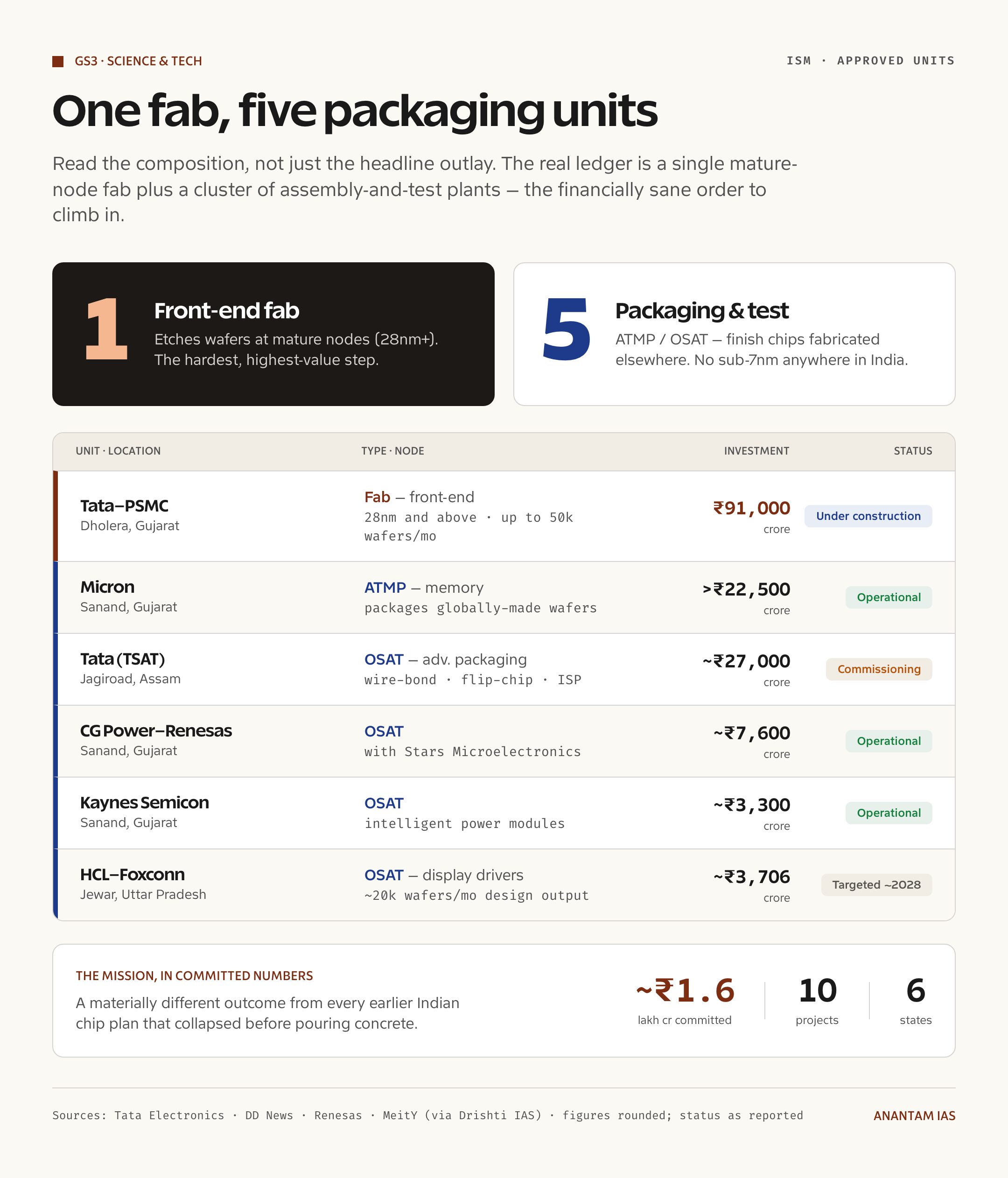
The numbers are where you slow down, because the money looks enormous until you see what it has actually bought, and what it hasn’t. Start with the mission itself. The Union Cabinet approved the India Semiconductor Mission in December 2021 with an outlay of ₹76,000 crore, about US$10 billion, offering fiscal support of up to 50 percent of project cost for fabs, packaging units, and design. By December 2025, that had pulled in 10 approved projects carrying cumulative investment commitments of roughly ₹1.6 lakh crore across six states. That’s the headline India keeps repeating, and it’s genuinely a different result from every earlier Indian chip plan that collapsed before pouring concrete.
Now read the composition, because it’s the spine of the whole topic. Of those committed projects, exactly one is a front-end fab: the Tata-PSMC plant at Dholera in Gujarat, up to ₹91,000 crore, capacity up to 50,000 wafers a month, at nodes of 28nm and above. The rest are packaging and test. Micron’s Sanand ATMP, more than ₹22,500 crore, inaugurated 28 February 2026, turns Micron’s globally-made memory wafers into modules. Tata’s own OSAT at Jagiroad in Assam, around ₹27,000 crore, is commissioning through 2026. CG Power’s joint venture with Renesas at Sanand, around ₹7,600 crore, is live. Kaynes Semicon, around ₹3,300 crore, went into production around 31 March 2026. HCL-Foxconn’s display-driver unit near Jewar in Uttar Pradesh, around ₹3,706 crore, is targeted for about 2028. So the real ledger reads: one mature-node fab plus five packaging and test units. There is no leading-edge, sub-7nm fab anywhere in the country.
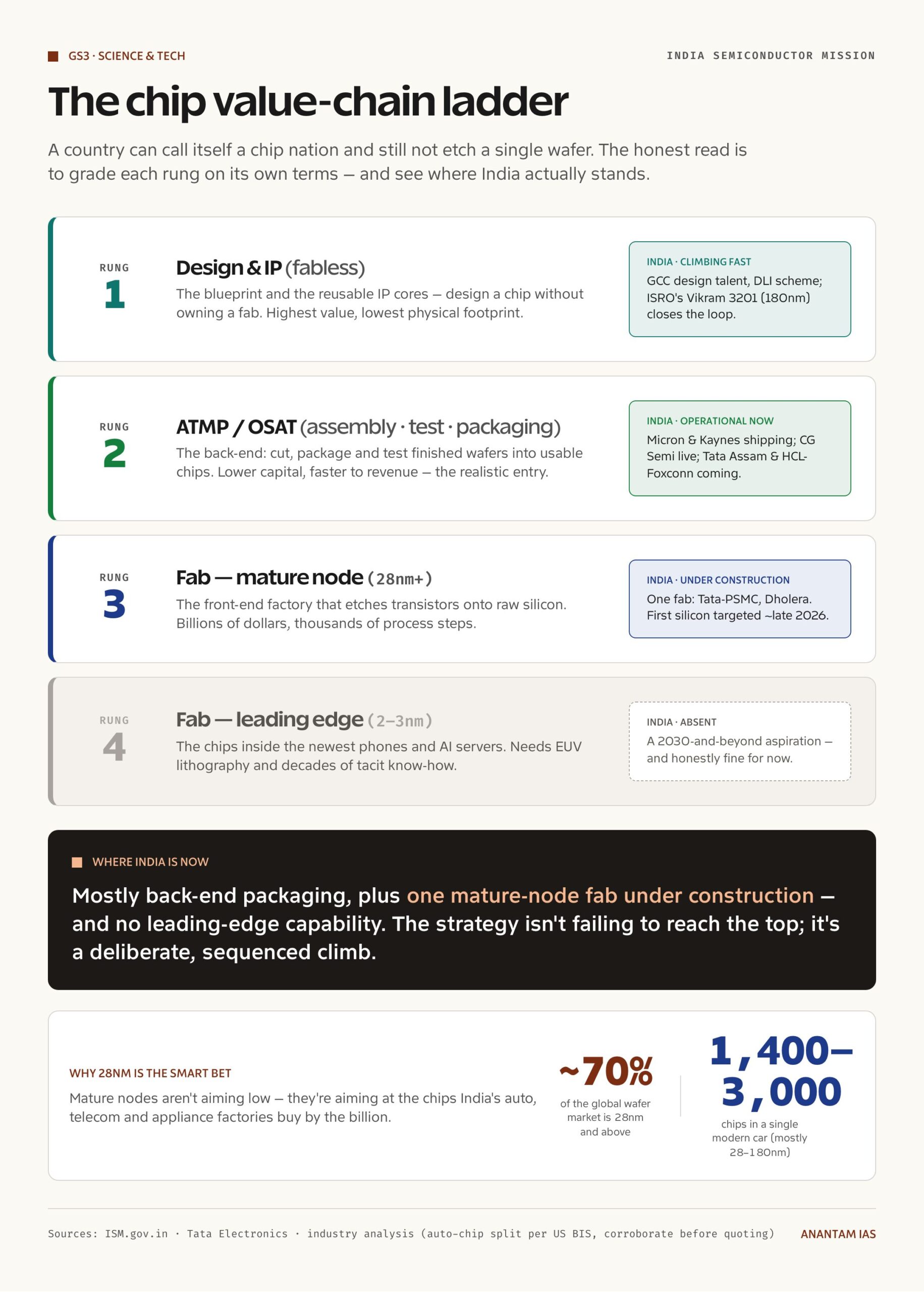
And that’s not the embarrassment it sounds like, which is the part most commentary gets wrong. Roughly 70 percent of the global wafer market sits at 28nm and above, and the chips that run a modern car overwhelmingly live between 28nm and 180nm, with a single vehicle carrying somewhere between 1,400 and 3,000 chips. So Dholera’s 28nm bet isn’t aiming low. It’s aiming at the chips India’s auto, telecom, and appliance factories actually buy by the billion.
The demand that justifies all of this is large and growing. India’s semiconductor market was roughly US$45 to 50 billion in 2024-25, projected toward US$100 to 120 billion by 2030, with a longer industry estimate of around US$300 billion by 2035 attributed to a Deloitte report rather than to government. Against that, India imports more than 90 percent of its chips today, with a stated roadmap to meet around 60 percent of demand domestically by 2035. So the offtake is real, which is exactly what earlier “build it and hope” attempts never had.
The Case For
The case for India’s approach is genuinely strong, and pretending otherwise would make for a lazy answer. So let’s state it at full strength.
It starts where the market actually is, not where the headlines are. Building a 28nm fab plus a cluster of packaging units isn’t timidity, it’s matching capacity to the chips the Indian economy buys. With roughly 70 percent of global wafer demand at mature nodes and most automotive chips between 28nm and 180nm, Dholera is pointed at real, durable demand rather than at a leading-edge race India can’t win this decade. So the strategy reads the market correctly.
Packaging is the right first rung, and it’s already paying out. Micron in February 2026 and Kaynes in March 2026 are shipping product, CG Power’s unit is live, and Tata’s Assam OSAT and HCL-Foxconn are coming. Back-end work is lower capital and faster to revenue than a fab, and it builds the workforce, the supplier base, and the operating discipline that any front-end factory will later need. So the sequence, packaging before fab, is the financially sane order to climb in.
The anchor demand is real and growing, which changes the economics. A market heading from US$45 to 50 billion toward US$100 to 120 billion by 2030 gives offtake that the abandoned Indian fab attempts of earlier decades simply never had. Electric vehicles, data centres, mobile manufacturing, and the broader electronics push under production-linked incentives all supply the pull. So this isn’t a factory hunting for customers. The customers already exist.
Design IP plays to India’s deepest strength. India already houses a large share of the world’s chip-design engineers inside multinational global capability centres, and the Design Linked Incentive scheme aims to convert that captive talent into Indian-owned IP, targeting 100 design firms with at least 20 scaling past ₹1,500 crore in revenue. ISRO’s Vikram 3201, India’s first indigenous 32-bit microprocessor unveiled in 2025, proves the design-to-fabrication loop can close domestically. So the highest-value, lowest-footprint rung is the one India is best placed to climb.
And ISM 2.0 is aimed at the right gaps. Funded in Budget 2026-27 with a first-year provision of around ₹1,000 crore for FY 2026-27, it deliberately shifts focus from attracting fabs to building indigenous equipment, materials, chemicals and gases, full-stack Indian design IP, industry-led R&D and skilling, and supply-chain resilience. That pivot shows the government has read the binding constraints correctly: the iceberg below the fab, not just the fab. So the second phase is pointed at the real problem.
The Case Against
Here’s what the celebration walks past. A chip ecosystem isn’t judged only by ribbon-cuttings. It’s judged by how much of the value, and how much of the strategic autonomy, actually stays in the country. On that test, the build has real holes.
Packaging is not sovereignty. Most of the operational units assemble and test chips that were fabricated elsewhere. Micron packages wafers made in its global fabs; HCL-Foxconn will package display drivers. Back-end work captures the thinner slice of the value chain, and it leaves the hardest, highest-value step, making the wafer, still offshore. So “chip nation” overstates what a packaging cluster delivers.
The leading-edge gap is structural, not a matter of a few more years of effort. India can design down to 2nm but cannot fabricate below 28nm. Leading-edge manufacturing needs extreme-ultraviolet lithography, which is effectively a single-supplier global monopoly, thousands of process steps, and decades of accumulated tacit know-how that doesn’t transfer in a technology agreement. So the leading edge is a 2030-and-beyond aspiration, and any answer that treats it as around the corner is wrong.
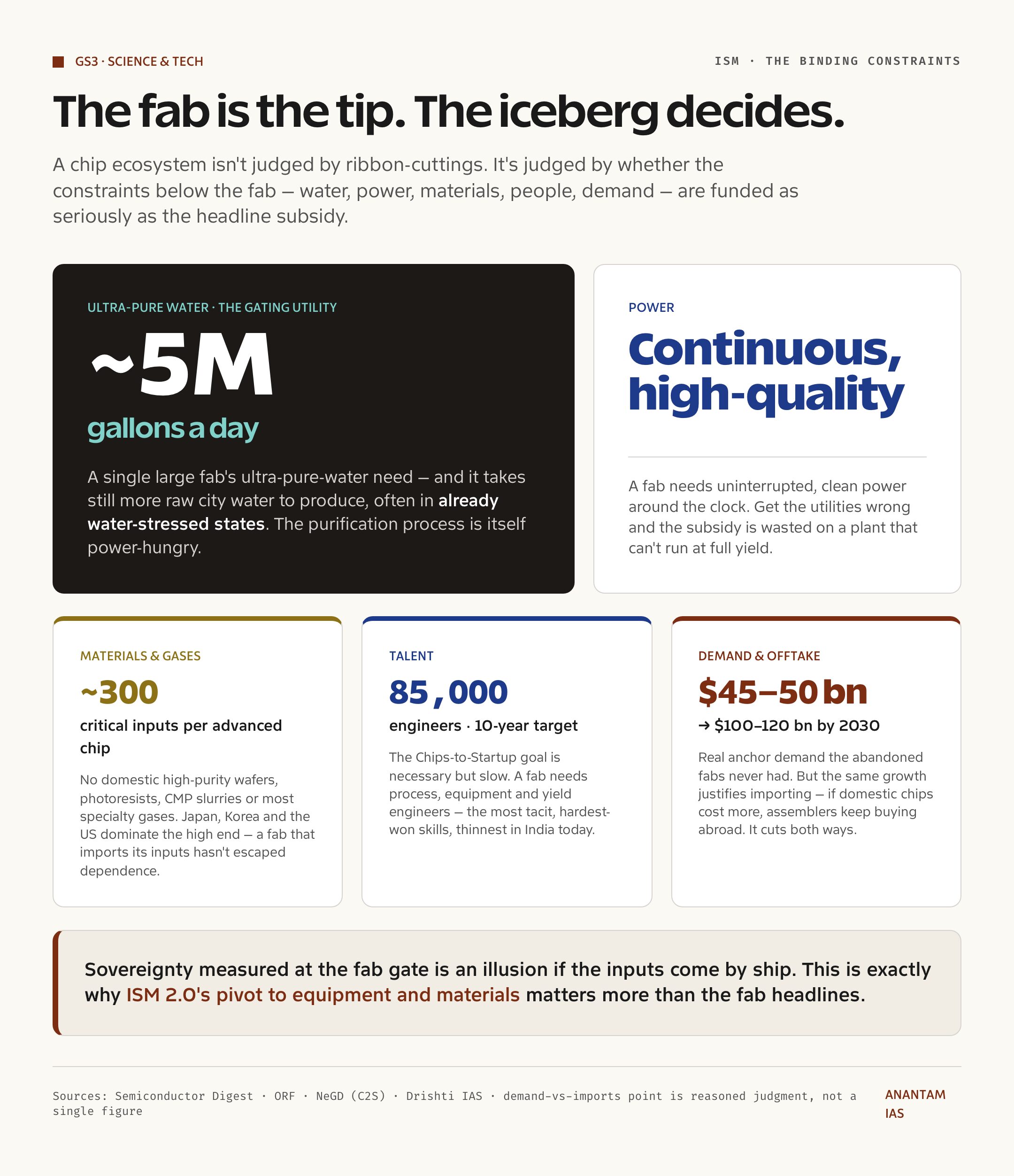
The materials, chemicals, and gases are the silent dependency, and they’re the part nobody photographs. India produces no domestic high-purity silicon wafers, and its supply of advanced photoresists, chemical-mechanical-polishing slurries, and most specialty gases is minimal to non-existent, with Japan, Korea, and the US dominating the high end. The most advanced chips draw on something like 300 critical inputs processed by around 50 classes of specialised equipment. So a fab that imports its inputs hasn’t escaped dependence. It has relocated one assembly step and kept the rest.
Water and power are physical, local, and contested. A single large fab can need around 5 million gallons a day of ultra-pure water, and producing that takes still more raw city water, in states that are often already water-stressed. The same fab needs continuous, high-quality power, and the ultra-pure-water process is itself power-hungry. So get the utilities wrong and the subsidy is wasted on a plant that can’t run at full yield.
Talent at scale is years away. The Chips-to-Startup programme targets 85,000 semiconductor engineers over 10 years, with design tools deployed across hundreds of institutions. But a fab needs more than designers. It needs process, equipment, and yield engineers, the most tacit and hardest-won skills in the industry, and those are thin in India today. So the talent pipeline is real but slow, and it lags the concrete.
And the economics can cut the other way. Up to 50 percent capital support is an extraordinary subsidy, and if global mature-node prices fall, which is plausible as large competitors flood 28nm capacity, Indian fabs could need recurring support to stay viable. The same market growth that justifies building also justifies importing, because if domestic chips cost more, India’s electronics assemblers will keep buying abroad unless protected. So the anchor-demand argument honestly cuts both ways.
The Deeper Structural Read
Step back from the ribbon-cuttings and the real fault line shows up. It isn’t “is India building chips or not.” It’s which rung of value India is capturing, and whether the sequence is honest. And the chip value chain already answers how the climb has to go.
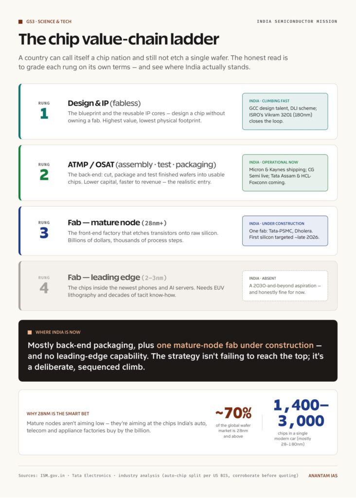
Think of four rungs. Design and IP at the top, where the blueprint and the margin live. Packaging and test below it, finishing chips made elsewhere. Mature-node fabrication below that, making the wafer at 28nm and above. And leading-edge fabrication at the bottom of the picture but the top of the difficulty, the 2nm-to-3nm work that a handful of firms on Earth can do. India is climbing fast on design, standing operational on packaging, under construction on the mature-node fab, and absent at the leading edge. Read in that order, the strategy isn’t a failure to reach the top. It’s a deliberate, sequenced climb, and the sequence is the smart part.
The trouble starts when rhetoric skips a rung. Call a packaging plant a fab, or imply a 2nm future is near, and you set an expectation the physics can’t meet, which is how good industrial policy gets branded a disappointment for not doing the impossible. So the analytical discipline an answer must show is to grade each rung on its own terms: packaging as a real, banked win; the mature-node fab as the genuinely hard next step; design IP as the highest-value bet; and leading-edge as honestly out of reach for now, and that being fine.
Here’s the part that should bother a future administrator most. The strongest technical argument for this whole build, that India can’t keep importing chips in a weaponised world, is exactly the argument that the materials layer never escaped. You can pour ₹91,000 crore into a fab and still depend on imported photoresist, slurry, and specialty gas to run it. So sovereignty measured at the fab gate is an illusion if the inputs come by ship. This is precisely why ISM 2.0’s pivot to equipment and materials matters more than the fab headlines, and why it deserves to be funded like it matters, not as a ₹1,000-crore footnote to a ₹76,000-crore mission.
There’s a capability-honesty layer underneath, too. Some near-term capacity leans on refurbished and legacy equipment, which is perfectly fine for mature nodes but is a ceiling on how deep the technology can go. So the question for the next decade isn’t whether India can run a 28nm line. It’s whether India builds the equipment and materials base that lets it ever climb past 28nm on its own terms, rather than renting the path each time.
What Should Be Done
So what does an honest climb actually look like? Not a slogan about self-reliance, but a sequence you could hand a policymaker tomorrow. Seven moves, in order, and none of them pretends the leading edge is near.
- Sequence the climb honestly: packaging and test, then mature-node fab, then design IP, then a niche at the leading edge, never skipping a rung. Bank the back-end wins first and stop overselling 2nm. The India Semiconductor Mission has, in practice, chosen this order already; the job now is to defend it against the temptation to claim more than the rung delivers.
- Fund the materials, chemicals, and gases base like it decides everything, because it does. Use India’s existing specialty-chemicals industry to localise photoresists, slurries, high-purity reagents, and specialty gases. This is exactly ISM 2.0’s first pillar, and it deserves a budget that matches its importance, not a fraction of what the fab subsidies command.
- Treat water and power as gating infrastructure, not afterthoughts. Dedicated ultra-pure-water plants with aggressive recycling, firm captive power including renewables, and utility planning built into the fab cluster from day one. Get this wrong and a 5-million-gallon-a-day fab in a dry district becomes a stranded asset.
- Build talent across the whole stack, not just the design layer. The 85,000-engineer target is necessary but not sufficient. Expand the institution network and tie it directly to the operating fabs and OSAT units as apprenticeships, so process, equipment, and yield engineers train on real lines, not just simulators.
- Back the design-IP and fabless layer hard. Convert the global-capability-centre design talent into Indian-owned IP through the Design Linked Incentive scheme. This is the highest-value, lowest-physical-footprint rung, and the one where India starts with a genuine head start rather than from zero.
- Pick a defensible niche instead of chasing the 2nm crown. Advanced packaging and chiplets, where multiple smaller dies are stitched into one high-performance package, plus compound semiconductors like silicon carbide and gallium nitride for power electronics. India can lead at the system level without winning the leading-edge race, and the demand is already there in EVs and grid hardware.
- Plan subsidy off-ramps and lock in demand anchors. Tie incentives to milestones and to committed offtake from government, telecom, automotive, and defence procurement, so fabs aren’t perpetually subsidy-dependent and so the “imports are cheaper” pressure has a domestic counterweight that isn’t just a tariff wall.
Every one of these is pro-build. None of them is leading-edge fantasy. A chip ecosystem climbed in order, with the materials base funded and the utilities solved, is one that actually compounds, rather than one that needs a fresh subsidy every time global prices wobble.
For Your Mains Answer
This is a clean GS3 topic. It maps to science and technology, indigenisation, achievements of Indians in S&T, and industrial and investment policy, with a light spillover into government interventions and technology partnerships.
GS paper mapping: GS3: Science and technology developments and applications; indigenisation of technology and developing new technology; effects of liberalisation and industrial policy; infrastructure and investment models. (Light GS2 spillover: government policies and interventions.)
Likely question frames:
- India’s semiconductor push is necessary but must be sequenced. Examine the rationale behind prioritising packaging and mature-node fabrication over leading-edge manufacturing.
- “A fab is the tip; the ecosystem is the iceberg.” Critically analyse the constraints that will decide the success of the India Semiconductor Mission.
- Discuss how the India Semiconductor Mission seeks to reduce import dependence in semiconductors, and assess the structural challenges that remain.
Quotable data points:
- ISM 1.0: ₹76,000 crore (about US$10 billion), approved December 2021, up to 50 percent fiscal support.
- ISM 2.0: about ₹1,000 crore for FY 2026-27, refocused on equipment, materials, chemicals and gases, design IP, R&D, and skilling.
- 10 projects, about ₹1.6 lakh crore committed across six states by December 2025.
- One front-end fab plus five packaging and test units; no sub-7nm capability in India.
- Tata-PSMC Dholera: up to ₹91,000 crore, up to 50,000 wafers a month, 28nm and above.
- More than 90 percent of India’s chip needs are imported today; target of about 60 percent domestic by 2035.
- Market about US$45 to 50 billion in 2024-25, heading toward US$100 to 120 billion by 2030.
- About 70 percent of the global wafer market sits at 28nm and above; most car chips are 28nm to 180nm.
- A single large fab can need about 5 million gallons of ultra-pure water a day.
- Chips-to-Startup target: 85,000 semiconductor engineers over 10 years.
Keywords to use: fab, ATMP, OSAT, mature node, 28nm, leading-edge, design IP, fabless, Design Linked Incentive, Chips-to-Startup, advanced packaging, chiplets, compound semiconductor, ultra-pure water, specialty gases, import dependence, value chain, Atmanirbhar.
Syllabus linkages: Science and technology developments and their applications, indigenisation of technology, achievements of Indians in S&T, industrial policy and investment models, infrastructure, government interventions.
Balanced conclusion line: India’s chip story is strongest when it’s honest about the ladder; sovereignty isn’t won at a single fab gate but built rung by rung, and the rung India is on, packaging proven and a mature-node fab rising, is a real beginning that the materials, water, power, and talent base now has to be funded to carry upward.
How to Build the Answer
Open with the tension, not a definition. The sharpest opening here is that a country can declare itself a chip nation and still not fabricate a single wafer from scratch, and that this gap is the actual subject. That first line tells the examiner you understand both the policy ambition and the technical reality. The definitions of fab, OSAT, and node can follow in the next sentence, where they earn their place rather than padding the intro.
Bring data in early, but ration it. A strong first body paragraph can carry three numbers: ₹76,000 crore for the mission, ₹1.6 lakh crore committed, and the composition of one fab plus five packaging units. Then say what the composition proves: that India is on rung one, not at the summit. The figure is the anchor; the “this means” is the mark.
Steelman both sides. If your stance backs the build, first concede the materials dependency and the leading-edge gap. If your stance is critical, first admit that 28nm is the smart bet and that packaging is the financially sane first rung. That’s how an answer reads balanced without going vague.
Group the way forward. Cluster the reforms into honest sequencing, materials base, gating utilities, full-stack talent, design IP, a defensible niche, and subsidy off-ramps. Use the topic’s own vocabulary, mature node, value chain, advanced packaging, so the answer sounds like industrial-policy analysis rather than a news recap.
Close on judgment, not a slogan. The reliable pattern is “sovereignty isn’t won at one fab gate; it’s built rung by rung,” which lets you balance ambition against constraint and end on a value the examiner can grade.
Common Mistakes to Avoid
- Don’t call every chip unit a “fab.” Most Indian units are OSAT or ATMP packaging. Conflating them with fabrication is the single most common error on this topic, and examiners notice it.
- Don’t claim the leading edge is near. India can design 2nm but can’t fabricate below 28nm. Treating sub-7nm as imminent shows you haven’t grasped the structural gap.
- Don’t go one-sided. This topic has a real counter-argument on both ends. Concede the strong case for mature-node and packaging before critiquing the sovereignty rhetoric, or vice versa.
- Don’t ignore the iceberg. An answer that lists fabs but skips water, power, materials, and talent has missed where success is actually decided.
- Don’t end on a flourish. Close with a sequenced principle or a named constraint, not “India is poised to become a chip superpower.”
A Compact Answer Spine
- Introduction: Open with the chip-nation-versus-no-fab tension; define fab, OSAT, and node in the next line.
- Evidence: Use the mission outlay, the committed investment, and the one-fab-five-packaging composition, each tied to an implication.
- Arguments: The case for sequencing and mature-node, then the case against the sovereignty overclaim and the materials gap. Keep both fair.
- Structural diagnosis: The four-rung value chain; India is capturing the lower-value rungs first, by design, and the materials layer is the real test.
- Way forward: Six to seven grouped moves, each with a clear actor, government, ISM, industry, states.
- Conclusion: Adapt the balanced conclusion line to the exact question wording.
Diagram or Flowchart Idea
For a 15-marker, draw the value-chain ladder as one vertical sequence: design and IP, then packaging and test, then mature-node fab, then leading-edge fab, with an India marker on each rung, strong on design, operational on packaging, under construction on mature-node, absent at the leading edge. The examiner reads the entire argument in five seconds.
For a 10-marker, skip the ladder and use a two-column “Strengths against Constraints” table, market demand and design talent on one side, materials dependency and utilities on the other. It’s faster to evaluate under time pressure and still shows you’ve grasped both halves.
Ethics and Governance Angle
Even a GS3 technology answer rewards one line on who bears the cost and who carries the risk. A 5-million-gallon-a-day fab in a water-stressed district raises a real distributive question: is scarce groundwater being routed to an export-oriented plant while nearby farms ration? Naming that tension, rather than waving it away, shows administrative maturity.
Then convert it into design. Don’t just say “balance industry and community.” Say how: ultra-pure-water recycling, captive renewable power, and transparent local water budgeting written into the clearance itself. That’s the move from moral language to governance you could actually implement.
A useful sentence travels across topics: “The policy is legitimate in aim, but its legitimacy depends on whether the constraints, water, power, materials, and talent, are funded as seriously as the headline subsidy.” It accepts the objective without handing the State a blank cheque.
How to Use Data Without Sounding Mechanical
Use fewer numbers than you know. Three well-placed figures beat ten scattered ones. Lead with one big anchor, ₹1.6 lakh crore committed. Use a second for the structure, one fab plus five packaging units. Use a third to justify the strategy, about 70 percent of the global wafer market at 28nm and above. One scale figure, one composition figure, one market figure is usually enough.
Never leave a statistic standing alone. Follow it with “this means” or “the implication is.” The 5-million-gallon water figure, for instance, only earns its place when you add that it makes utilities a gating constraint, not a footnote. That tiny move turns a fact sheet into analysis.
Finish by asking one question: can a tired examiner follow this in a single pass? If a sentence sounds impressive but does no work, cut it and replace it with a fact, a cause, a consequence, or a reform. For UPSC, clarity is how depth becomes visible. Always be specific.
FAQ
What is the difference between a fab and an OSAT or ATMP unit?
A fab, or fabrication plant, is the front-end factory that etches transistors onto a raw silicon wafer; it is capital-intensive and the technically hardest step. An OSAT, or ATMP, unit is the back-end that takes finished wafers and assembles, packages, and tests them into usable chips. Most of India’s operational semiconductor units are OSAT or ATMP packaging, with only the Tata-PSMC Dholera plant being an actual front-end fab, and even that is at mature nodes rather than the leading edge.
Does India make leading-edge chips yet?
No. India can design chips down to 2nm, but it cannot fabricate anything below 28nm. The Dholera fab targets 28nm and above, which is mature-node territory. Leading-edge manufacturing at 2nm to 3nm needs extreme-ultraviolet lithography, thousands of process steps, and decades of tacit know-how, so it remains a 2030-and-beyond aspiration for India, not a current capability, and that is a reasonable place to be for now.
Why focus on 28nm instead of the most advanced chips?
Because that’s where the market is. Roughly 70 percent of the global wafer market sits at 28nm and above, and most chips inside cars, appliances, and industrial systems are between 28nm and 180nm. Building for mature nodes matches India’s actual demand from its automotive, telecom, and electronics sectors, and it’s a far more achievable and financially sustainable target than racing for a leading edge a handful of firms on Earth can reach.
What does ISM 2.0 change compared with ISM 1.0?
ISM 1.0, approved in December 2021 with a ₹76,000-crore outlay, focused on attracting fabs and packaging units with up to 50 percent capital support. ISM 2.0, funded in Budget 2026-27 with a first-year provision of about ₹1,000 crore, shifts the focus to the layers underneath the fab: indigenous equipment, materials, chemicals and gases, full-stack Indian design IP, industry-led R&D and skilling, and supply-chain resilience. In short, ISM 1.0 built the factory; ISM 2.0 tries to build the ecosystem that keeps it running on Indian terms.
Tell Google you want more of this.
Add Anantam IAS as a preferred sourceOne tap, and this site shows up more often in your own Top Stories, AI Overviews and AI Mode. Remove it any time.