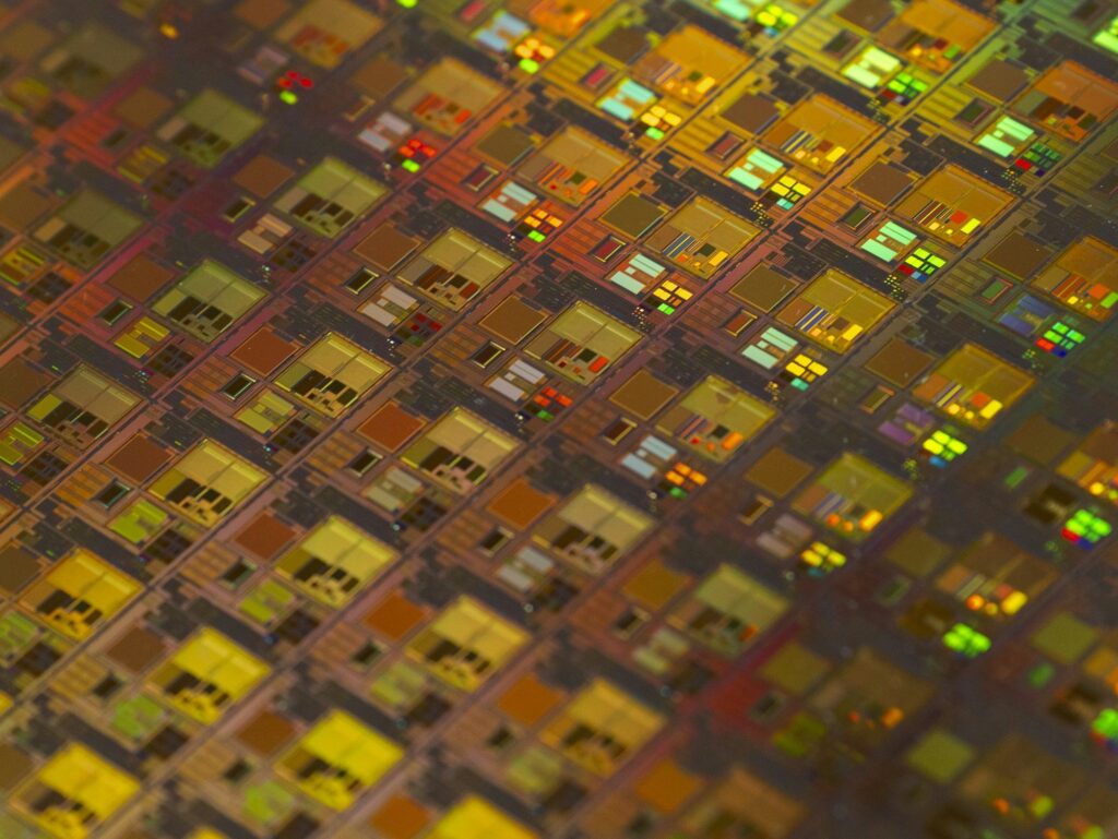
The India Semiconductor Mission is the Government of India’s flagship programme to build a domestic semiconductor design, fabrication, packaging and equipment ecosystem within this decade. Approved by the Union Cabinet on 15 December 2021 with an initial outlay of ₹76,000 crore and operationalised under the Ministry of Electronics and Information Technology (MeitY), the India Semiconductor Mission is the largest single industrial-policy push the country has ever made in the electronics sector. By mid-2026 the mission has approved six semiconductor projects with a combined investment of over ₹1.6 lakh crore, including Micron Technology’s assembly and test plant at Sanand, the Tata-PSMC fab at Dholera, the CG Power-Renesas-Stars ATMP at Sanand, the Tata Electronics OSAT at Jagiroad, the Kaynes Technology unit at Sanand and the HCL-Foxconn display-driver IC fab at Jewar. The India Semiconductor Mission is closely linked to other technology programmes such as the green hydrogen mission, solar PLI, electric vehicle drive and battery technology push that together aim to redraw India’s manufacturing map.
Why Semiconductors Matter
Semiconductors are the basic building blocks of every modern electronic device — from smartphones and laptops to cars, satellites, fighter jets, medical equipment and the chips that train large language models. India imports almost the entirety of its chip requirement, which is set to reach over $110 billion by 2030 as electronics manufacturing scales up. The COVID-19 pandemic exposed how fragile concentrated chip supply chains are: a shortage of automotive microcontrollers in 2021-22 forced Indian carmakers to cut production by 20-25%. Building domestic capability is therefore both an industrial-policy goal and a national-security imperative.
The Global Chip Landscape
Around 75% of global wafer fabrication capacity sits in East Asia — Taiwan (TSMC), South Korea (Samsung, SK Hynix), China and Japan. The United States, Europe and India have all responded with massive subsidy programmes — the US CHIPS and Science Act ($52.7 billion), the European Chips Act (€43 billion), and India’s own ₹76,000 crore semiconductor scheme.
Origins of the India Semiconductor Mission
India’s semiconductor journey has older roots. The Semiconductor Complex Limited (SCL) at Mohali was set up in 1976 but lost ground after a fire in 1989. Earlier attempts to attract foreign fabs — including a 2007 plan involving SemIndia — fell through. The current mission learns from those failures by offering up-front capital subsidies, fiscal incentives and infrastructure support rather than just market-access promises.
The Union Cabinet approved the modified Semicon India programme on 21 September 2022 with the following four components:
- Modified Scheme for Setting up of Semiconductor Fabs — up to 50% fiscal support of project cost.
- Modified Scheme for Display Fabs — up to 50% fiscal support.
- Modified Scheme for Compound Semiconductors, Silicon Photonics, Sensors and ATMP/OSAT — 50% capex support.
- Design Linked Incentive (DLI) Scheme — for fabless design startups.
The India Semiconductor Mission, set up as an Independent Business Division within Digital India Corporation, executes the programme.
Approved Fabs and Projects
By mid-2026 the India Semiconductor Mission has approved six projects with combined committed investment of over ₹1.6 lakh crore.
Micron Technology — Sanand, Gujarat
Approved in June 2023, Micron’s $2.75 billion ATMP (Assembly, Testing, Marking and Packaging) plant at Sanand, Gujarat, is the first ISM-supported facility to break ground. The Government of India provides 50% capex support and Gujarat adds another 20%. Phase 1 will begin packaging operations in late 2025 with DRAM and NAND memory chips for global Micron supply chains.
Tata-PSMC — Dholera, Gujarat
Approved in February 2024, the Tata Electronics joint venture with Taiwan’s Powerchip Semiconductor Manufacturing Corporation (PSMC) at Dholera Special Investment Region is India’s first commercial wafer fabrication unit, with a planned investment of ₹91,000 crore for 50,000 wafer starts per month at 28 nm process node. The fab will serve automotive, consumer electronics and industrial applications.
CG Power-Renesas-Stars — Sanand, Gujarat
The CG Power joint venture with Renesas Electronics of Japan and Stars Microelectronics of Thailand will build a ₹7,600 crore OSAT (Outsourced Semiconductor Assembly and Test) facility at Sanand for specialised power-management ICs.
Tata Electronics OSAT — Jagiroad, Assam
A ₹27,000 crore OSAT/ATMP facility at Jagiroad in Assam — India’s first semiconductor unit in the Northeast, expected to begin production by 2025-26 and create over 27,000 direct and indirect jobs.
Kaynes Semicon — Sanand, Gujarat
A ₹3,300 crore ATMP unit by Kaynes Technology at Sanand, approved in September 2024.
HCL-Foxconn — Jewar, Uttar Pradesh
A ₹3,706 crore joint venture between HCL Group and Foxconn approved in May 2025 to manufacture display-driver ICs (DDIC) at the Yamuna Expressway Industrial Development Authority area near Jewar. This is the first ISM project outside Gujarat-Assam.
Aggregate Investment
Total committed investment across these six projects exceeds ₹1.6 lakh crore. Cumulative jobs creation potential is over 80,000 direct and several lakh indirect roles in construction, materials, supply chain and design services.
Design Linked Incentive Scheme
The Design Linked Incentive (DLI) scheme has a ₹1,000 crore outlay and supports Indian semiconductor design start-ups across three components — Chip Design Infrastructure Support, Product Design Linked Incentive (up to 50% of project cost) and Deployment Linked Incentive. By 2026 over 40 DLI start-ups have been onboarded across areas like microprocessors, FPGAs, RF chips, AI accelerators and sensors. The Centre for Development of Advanced Computing (C-DAC) manages the operational rollout.
ChipIN Centre
The ChipIN Centre is a “one-stop” facility set up by C-DAC under the DLI scheme to give start-ups access to commercial EDA (Electronic Design Automation) tools, foundry shuttle services and packaging support. It dramatically lowers the upfront cost of chip design for early-stage firms.
Other Schemes That Reinforce ISM
The India Semiconductor Mission does not work in isolation. Three additional schemes reinforce it.
Modified Special Incentive Package Scheme (M-SIPS)
The original M-SIPS gave 20-25% capex subsidy for electronics manufacturing units between 2012 and 2018 — its successor PLI scheme for electronic components and semiconductors is the current vehicle for component manufacturing.
Production Linked Incentive for Large-Scale Electronics
The ₹40,995 crore PLI for large-scale electronics manufacturing has anchored mobile phone assembly in India, scaling exports past $20 billion in 2024-25.
PLI for IT Hardware
The PLI for IT hardware (laptops, tablets, servers, all-in-one PCs) was approved with ₹17,000 crore. Approved beneficiaries include Dell, HP, Lenovo, Asus, Acer and Foxconn.
India Semiconductor Research Centre
Announced in Union Budget 2025-26, the proposed India Semiconductor Research Centre will partner with Indian Institutes of Technology and global R&D labs to build sovereign capability in next-generation nodes, advanced packaging and post-silicon technologies.
Talent and Skilling
A 28 nm fab requires roughly 1,000-1,500 trained engineers per shift. The mission’s talent strategy includes the Chips to Startup (C2S) programme with 113 academic institutions, the Skill India Future Skills Prime portal, and dedicated MTech programmes at IITs and IIITs in semiconductor technology and VLSI design. Tata Electronics, Micron and others are setting up in-house training academies in Gujarat and Assam.
Strategic Importance
The India Semiconductor Mission is strategic on three counts.
- Economic. India’s electronics market will cross $300 billion by 2030. Capturing even 25% of chip demand domestically saves $25-30 billion in imports per year.
- National security. Defence platforms — radar, missiles, fighter aircraft and satellites — increasingly depend on cutting-edge silicon. Strategic autonomy requires at least some sovereign fabrication.
- Geopolitics. India is positioning itself as the “China + 1” destination for global chip supply chains, working with US, Japanese, Taiwanese and European partners through frameworks like the Quad’s Semiconductor Supply Chain Initiative and the India-US iCET partnership.
Challenges and Bottlenecks
The mission faces several real challenges.
- Process technology gap. India’s first commercial fab will operate at 28 nm. Leading-edge fabs in Taiwan and South Korea are at 3 nm and headed to 2 nm.
- Ecosystem depth. A modern fab requires hundreds of suppliers — silicon wafers, photoresists, ultra-pure gases, photomasks, EUV-related materials. Most are imported.
- Water and power. A single 28 nm fab consumes 10-15 million litres of ultra-pure water per day and 100+ MW of electricity. Gujarat has invested in dedicated infrastructure but the long-term sustainability question remains.
- Talent supply. India has strong design talent but far fewer engineers with hands-on fab and equipment experience. Building that workforce will take a decade.
- Cyclical industry. Memory pricing in particular is sharply cyclical, which can squeeze early returns and test policy commitment across electoral cycles.
Way Forward
The India Semiconductor Mission has moved from policy announcement to ground-breaking faster than most observers expected. The next phase requires four moves: a second-tranche ₹76,000 crore extension to anchor compound semiconductors and advanced packaging, depth in upstream materials and equipment, a credible R&D push at the proposed India Semiconductor Research Centre, and consistent state-level facilitation around water, power and skilling. If these align, India can credibly emerge as a top-five global semiconductor packaging and mature-node fabrication hub by 2030.
Frequently Asked Questions
What is the India Semiconductor Mission?
The India Semiconductor Mission is a Government of India programme launched on 15 December 2021 with a ₹76,000 crore outlay to build a domestic semiconductor and display fabrication ecosystem. It is implemented as an Independent Business Division within Digital India Corporation under MeitY.
Which fabs have been approved under the India Semiconductor Mission?
Six projects have been approved — Micron at Sanand, Tata-PSMC at Dholera, CG Power-Renesas-Stars at Sanand, Tata Electronics OSAT at Jagiroad in Assam, Kaynes Technology at Sanand and HCL-Foxconn at Jewar in Uttar Pradesh.
What is the total investment committed under the mission?
Combined committed investment across the six approved projects exceeds ₹1.6 lakh crore.
What is the Design Linked Incentive scheme?
The DLI scheme has a ₹1,000 crore outlay and supports Indian semiconductor design start-ups through chip design infrastructure, product-development incentives and deployment incentives. Over 40 start-ups have been onboarded by 2026.
What is the ChipIN Centre?
The ChipIN Centre is a one-stop facility set up by C-DAC that gives Indian start-ups access to commercial EDA tools, foundry shuttle services and packaging support at subsidised rates.
Why is the India Semiconductor Mission strategically important?
Semiconductors underpin everything from smartphones and cars to defence platforms and AI infrastructure. Domestic fabrication reduces import dependency, secures defence supply chains and lets India participate in global u0022China + 1u0022 strategies.
What process node will the first Indian fab use?
The Tata-PSMC fab at Dholera will produce wafers at the 28 nm process node — suitable for automotive, consumer and industrial applications. Leading-edge global fabs are at 3 nm and below.
What are the main challenges for the mission?
Process-technology gap with global leaders, shallow upstream ecosystem for materials and equipment, water and power intensity, shortage of fab-experienced talent and industry cyclicality are the main challenges.
Tell Google you want more of this.
Add Anantam IAS as a preferred sourceOne tap, and this site shows up more often in your own Top Stories, AI Overviews and AI Mode. Remove it any time.